Configure Multi-Tile Synchronization on RFSoC Devices
This example shows how to use Multi-Tile Synchronization (MTS) for Zynq® UltraScale+™ RFSoC devices to ensure consistent timing and alignment between tiles and across devices. The Zynq® UltraScale+™ RFSoC features a flexible clock and data interface, allowing each RF analog-to-digital converter (ADC) and digital-to-analog converter (DAC) tile to operate with independent sample rates and data widths. Within a tile, all converters share the same clock and data path, resulting in fixed sample rates and latency. However, when applications require multiple tiles or devices, it is essential to synchronize latency across them.
The use of MTS enables precise alignment across tiles and devices to meet these requirements. It resolves latency differences by detecting timing mismatches between tiles and applying sample delays, ensuring all data streams are properly aligned.
This example demonstrates:
How to set up hardware for MTS on an RFSoC platform.
How to configure a model to use MTS in direct loopback applications
How to test your design on an RFSoC platform.
How to set up the digital local oscillator when using MTS.
How to configure MTS for non-direct loopback applications.
Requirements
Vivado® Design Suite. For a list of supported versions, see Supported EDA Tools and Hardware.
AMD Zynq UltraScale+ RFSoC ZCU111, ZCU2028, or ZCU216 evaluation kit.
HDL Coder Support Package for AMD FPGA and SoC Devices. Download the Linux image of the hardware board onto the SD card by using the Hardware Setup add-on. See Guided Hardware Setup for AMD Boards.
Use a Vivado version that corresponds to the PetaLinux® version of the RFSoC device you are using for the best results.
Configure RFSoC Board for Direct Loopback
In direct loopback configurations, the RF-ADC outputs directly feed the RF-DAC inputs, either within the same tile or across different tiles. Using MTS keeps the loopback path aligned by maintaining a consistent latency and phase.
To test your design on hardware intended for direct loopback applications, follow these steps:
Prepare Cables for use with MTS
This example will connect the cables so that they create a data path that bypasses the analog RF cage filter, which can introduce phase delays across different channels. To minimize noise, use differential cables with DC Blockers connected to one end to connect the differential ports on the RFSoC Boards. Additionally, to ensure accurate sample alignment measurements, avoid using mismatched cable types or filters that could alter signal timing.
Connect tiles on the ZCU111 board
For the ZCU111 connect the ADC and DAC channels using the differential SMA ports on the XM500 balun card. Specifically connect:
DAC 00 to ADC 04
DAC 01 to ADC 07
Since tile connections use 0-based indexing, these connections represent:
DAC Tile 0 Channel 0 connecting to ADC Tile 2 Channel 0
DAC Tile 0 Channel 1 being connected to ADC Tile 3 Channel 2
By connecting different tiles on the balun cards, the boards can compare the output from the channels on these different tiles for synchronization. The figures below show the ADC and DAC connections on ZCU111 boards.


Connect DACs with ADCs on the ZCU216 board
For the ZCU216, connect the ADC and DAC channels using the XM655 balun card. For this board, connect:
DAC P/N 0_228 to ADC P/N 02_224
DAC P/N 0_229 to ADC P/N 00_225
The specific headers that should be connected on the balun card are shown in the following figures:


These header connections represent:
DAC Tile 0 Channel 0 being connected to ADC Tile 0 Channel 2
DAC Tile 1 Channel 0 being connected to ADC Tile 1 Channel 2
The figures below show the ADC and DAC connections on ZCU216 boards.


For the ZCU208 board, connect the ADC and DAC channels using the XM655 balun card. For this board, connect following channels using a DC block:
DAC Tile 0 Channel 0 to ADC Tile 0 Channel 0
DAC Tile 1 Channel 0 to ADC Tile 1 Channel 0
For more information on setting up cable connections, see the AMD documentation for the respective board.
SYSREF Signal Requirement
The SYSREF signal is the timing reference signal for the system and must be set correctly to avoid degrading synchronization. Using MTS on the Xilinx® Zynq UltraScale+ RFSoC ZCU111, Xilinx Zynq UltraScale+ RFSoC ZCU208, and Xilinx Zynq UltraScale+ RFSoC ZCU216 evaluation kits require selecting specific sample rates governed by SYSREF signals from an external clock.
According to Xilinx datasheet PG269, the SYSREF frequency must meet these requirements:
To synchronize RF-ADC and RF-DAC tiles with different sample frequencies, the SYSREF frequency must be an integer sub-multiple of
GCD(DAC_Sample_Rate/16, ADC_Sample_Rate/16).To ensure the periodic SYSREF samples synchronously, the SYSREF frequency must be an integer sub-multiple of the PL clocks that sample it.
The SYSREF value must be less than 10 MHz.
On the ZCU111 board, the default SYSREF frequency produced by the LMK is 7.68 MHz. To meet SYSREF frequency requirements, the MTS models use ADC and DAC sampling rates of 1966.08 MHz, which is an integer multiple of this SYSREF frequency.
Many designs select a reference clock to satisfy SYSREF frequency requirements. For the ZCU111, ZCU208, and ZCU216 boards, the reference clock must be an integer multiple of the SYSREF frequency. For example, 245.76 MHz is a common choice for the ZCU208 and ZCU216 boards. For the ZCU111 board, designs typically use the external phase-locked loop (PLL) reference clock rather than the internal clock.
Open Example Project
This example shows how to use MTS to align channel samples across different tiles on the ZCU111, ZCU208, and ZCU216 boards. To get started, open the example project and copy the provided files to a temporary directory.
1. Navigate to the example source folder by entering these commands:
example_root = (hdlcoder_rfsoc_examples_root)
cd (example_root)
Make sure, you have installed the HDL Coder Support Package for AMD FPGA and SoC Devices. For more information, see Download and Install HDL Coder Support Package for AMD FPGA and SoC Devices
2. Copy the example files in the MTS folder to a temporary folder.
3. Add the temporary folder to the MATLAB Path
The example project includes MTS models along with the necessary support files to configure the model for to leverage MTS.
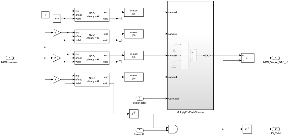
Model Description
This example provides two models, rfsoc_zcu216_MTS_iq_HDL.slx and rfsoc_zcu111_MTS_iq_HDL.slx, which represent the models that connect to the ZCU216 and the ZCU111 boards, respectively. You can also use the rfsoc_zcu216_MTS_iq_HDL model for the ZCU208 board. Both models implement the same algorithm, but differ in their interface mappings and ports configurations, targeted specifically for their respective board.
Open the rfsoc_zcu216_MTS_iq_HDL.slx model by calling the following command.
open_system('rfsoc_zcu216_MTS_iq_HDL.slx')After this, open the ADC_DAC_8x8_IQ_MTS_Capture subsystem.

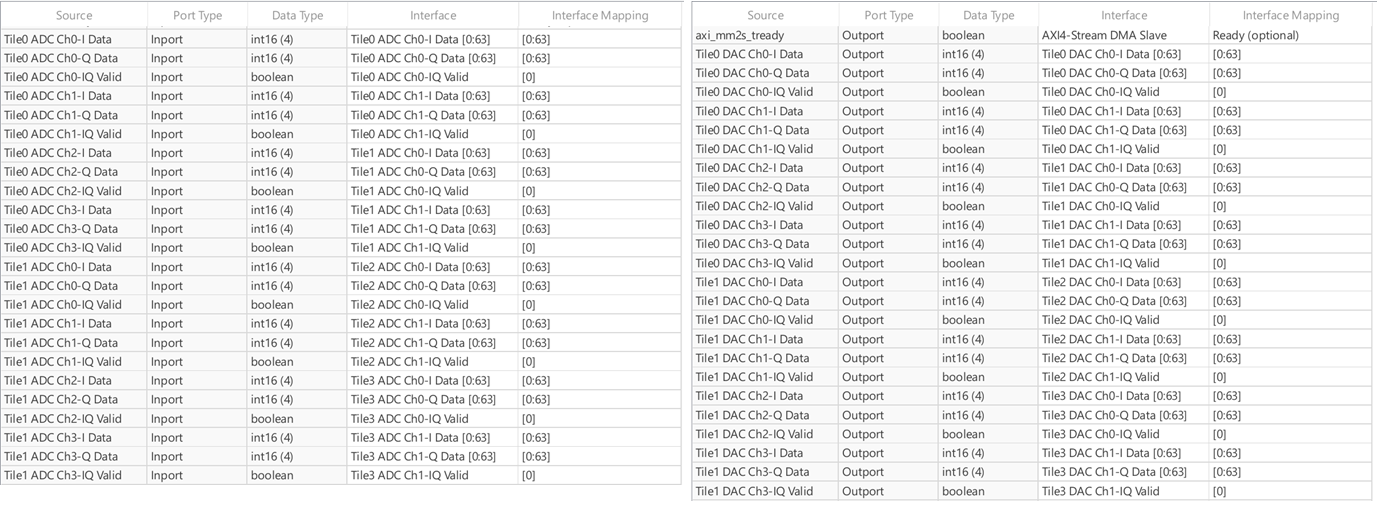
The algorithm captures data using two channels, selected through an AXI4 register that controls routing. A frame size and data capture trigger register manage the transfer of data to direct memory access (DMA) accordingly. A multiplexer (MUX) allows selection between inphase (I) or quadrature (Q) components for channel comparison. Since the design processes four IQ samples per clock cycle, the available data width for channel transfer is limited.
The models are configured so that the DAC tiles does not transmit output until the StreamEn signal is asserted. This delay allows the RF Data Converter additional time to complete any required synchronization. Open the NCO_Transmit subsystem to see how the model gates the StreamEn signal based on data transmission.
Generate HDL Code and Synthesize the Bitstream
Open the model associated with your board. To generate HDL code and program RFSoC board, follow these steps:
1. Select Apps tab on the Simulink toolstrip and select HDL coder. The HDL Code tab will appear on the Simulink toolstrip.
2. Select the ADC_DAC_8x8_IQ_MTS_CAPTURE subsystem and then click Workflow Advisor in the HDL Code tab.
3. In step 1.1 of the HDL Workflow Advisor, set the Target Workflow to IP Core Generation and Target Platform to Xilinx Zynq UltraScale+ RFSoC ZCU111 Evaluation Kit, Xilinx Zynq UltraScale+ RFSoC ZCU208 Evaluation Kit, or Xilinx Zynq UltraScale+ RFSoC ZCU216 Evaluation Kit, depending on the model you choose.
4. In step 1.2, set these values for the reference design parameters:
AXI4-Stream Master data width to
128AXI4-Stream Slave data width to
128Add external memory access (AXI4 Master) to
falseADC sampling rate (MHz) to
1966.08ADC decimation mode (xN) to
4ADC samples per clock cycle to
4ADC mixer type to
FineDAC sampling rate (MHz) to
1966.08DAC interpolation mode (xN) to
4DAC samples per clock cycle to
4DAC mixer type to
FineADC/DAC NCO mixer LO (GHz) to
0Enable multi-tile sync to
true
5. If you are using a ZCU208 or ZCU216 board, additionally set the DAC DUC mode parameter to Full DUC Nyquist (0-Fs/2).
6. In step 1.3, if you are using a ZCU208 board, for the DAC and ADC ports, set the target interface as shown in the image.
7. In step 4.2, to generate a script that provides MATLAB connectivity to the board for interactive testing and live I/O interfacing, select Generate host interface script and clear the Generate Simulink software interface model checkbox.
8. Run all HDL Workflow Advisor tasks to build the bitstream and then program the hardware board.
Test MTS Alignment
After setting up the board connections and programming the RFSoC board, you can test the effectiveness of MTS. The MTS example folder contains data capture scripts named:
HostIO_rfsoc_zcu111_MTS_iq_HDL_interface.m(for the ZCU111 Board)
HostIO_rfsoc_zcu216_MTS_iq_HDL_interface.m(for the ZCU216 Board)
To verify channel alignment across different channels, run the data capture script corresponding to your board. In the MATLAB command window enter one of the following commands.
HostIO_rfsoc_zcu111_MTS_iq_HDL_interface
Or
HostIO_rfsoc_zcu216_MTS_iq_HDL_interface
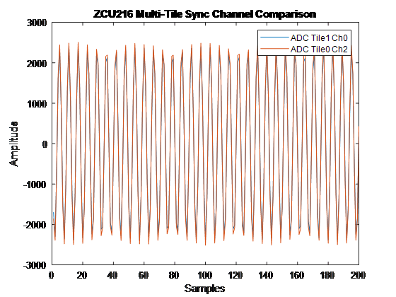
The graph above shows the result of data capture from a ZCU216 board for two channels, ADC Tile 1 Channel 0 and ADC Tile 0 Channel 2. It demonstrates near-perfect alignment between the channels.
Configure Digital Local Oscillator
While running MTS, you must not change the digital local oscillator (LO) frequency on the RFSoC. The LO of each channel may not be time-aligned, which can cause misalignment between channels. The RFSoC provides ways to deal with this by synchronizing the reset condition on all channels based on tile events. By configuring the tile events to respond to a SYSREF signal, you can achieve time alignment when using the mixer and LO frequency during MTS.
In this example, the reference design parameter ADC/DAC NCO mixer LO(GHz) is set to 0 to avoid LO alignment issues from impacting the direct cable loopback. To modify the LO frequency, first disable SYSREF capture, make the necessary changes to the LO frequency, and then re-enable SYSREF.
The example provides a script named ZCU216_ChangeLO.m or ZCU111_ChangeLO.m, which demonstrates this process. Run the script corresponding to your board to adjust the LO frequency.
MTS Configuration for Non-Loopback Applications
When you configure MTS for a direct cable loopback, the data channels are well aligned without accounting for the channel latency. For applications other than direct cable loopback, you must consider channel latency for better synchronization.
To configure MTS with channel latency, follow these steps:
1. Determine the latency of the channels on each tile by using the RFTool. Add the following commands in the RF_Init.cfg file located in the SD card.
MTS_Sysref_Config 1 3 15
MultiConverter_Sync 1 -1 3
MultiConverter_Sync 0 -1 15
MTS_Sysref_Config 0 3 15
MTS_Sysref_Config uses one-hot decoding to control which tiles are enabled. The commands assume the configuration of all 2 DAC Tiles and 4 ADC Tiles available on the ZCU111. The commands assume the configuration of all 2 DAC Tiles and 4 ADC Tiles available on the ZCU111. Passing in the 3 indicates to the RFTool to configure the first 2 DAC tiles. Passing in the 15 indicates to the RFTool to configure all 4 ADC tiles.
Reboot the board and observe the output captured in the rf_init.log file available on the SD card.
2. Calculate the target latency that must be set for the channels. The target latency is calculated by adding an appropriate margin value to the latency value obtained from step 1. For more information on how to determine target latency for channels, see Deterministic Multi Tile Synchronization API Use on the AMD website.
DAC_Latency: "MultiConverter_Sync 1" return latency + Margin
ADC_Latency: "MultiConverter_Sync 0" return latency + Margin
3. Specify the target latency by adding the following commands into the RF_Init.cfg file. Insert the SD card on the board and reboot the board to apply these settings to the board.
MTS_Sysref_Config 1 3 15
MultiConverter_Sync 1 <DAC_Latency> 3
MultiConverter_Sync 0 <ADC_Latency> 15
Each time the board is powered off, the target latency calculated in step 2 changes. This is because the return latency obtained from step 1 can change each time you power on the board.