Read and Write EEPROM Using SPI blocks on STM32 Microcontroller
This example shows how to use Serial Peripheral Interface (SPI) blocks provided in the STM32 Microcontroller Blockset to interface between an SPI bus and a Microchip 25XX080 8K SPI Bus Serial EEPROM. This EEPROM is organized as a 1024×8-bit (1024 bytes) memory device with a 16-byte page size.The example explains EEPROM module concepts and covers how to:
Set up hardware connections
Configure the microcontroller SPI peripheral
Read and Write EEPROM Data Using SPI Controller Transfer Block
Read and Write EEPROM Data Using SPI Transmit and Receive Blocks
Prerequisite
Complete the following tutorial:
Required Hardware
Available Models
spiEEPROMWithControllerTransferBlock.slx - Read and Write EEPROM Data Using SPI Controller Transfer Block
spiEEPROMWithReceiveTransmitBlock.slx - Read and Write EEPROM Data Using SPI Receive and Transmit Block
EEPROM Module Concepts
Memory Layout and Addressing
The Microchip 25XX080 8K SPI Bus Serial EEPROM module has 8Kbits of memory (1024 bytes) and requires 10 bits (A0 to A9) to address the entire memory space. The SPI protocol for the device requires a 16-bit address for data transmission.
Valid address range: 0x0000to0x03FF(0to1023accounting for 1024 bytes)Address transmission: 16-bit address is split into two bytes
High byte (MSB): Contains Don't Care bits (
A15toA10) and the two highest physical address bits (A9 andA8)Low byte (LSB): Contains the lower 8 physical address bits (
A7 toA0)
To address 0x0200:
Transmit MSB:
0x02(0b0000 0010)Transmit LSB:
0x00(0b0000 0000)
The memory is divided into 16-byte pages. Writes must not cross page boundaries in a single operation. When writing multiple bytes (for example, the address increments past 0bxxxx 1111), the internal address counter rolls over to the start of the same page, overwriting previous data. To write to contiguous memory across page boundaries, for each page, increment the address by 0x10 (16 decimal) and then perform a write operation.
This table, from the Microchip 25XX080 8K SPI Bus Serial EEPROM datasheet, shows the module instruction set.
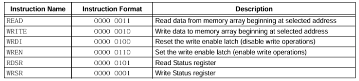
Write to EEPROM
To write to the EEPROM:
1. Set the write enable latch with the WREN instruction by completing this write enable sequence:
Drive chip select (CS) line low > Send 0x06 > Drive CS line high
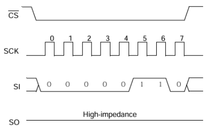
If you do not set the write enable latch (WEL) or toggle the CS line, a silent failure occurs.
2. Initiate a write operation with the WRITE instruction by completing this page write sequence:
Drive CS line low > Send 0x02 (WRITE) > Send 16-bit Address > Send Data (Max 16 bytes) > Drive CS line high after data byte is transferred
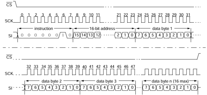
3. Trigger a write cycle.
To write data to memory, drive the CS line high after the least significant bit (D0) of the last most data byte has been clocked in. Otherwise, the write operation does not complete.
The Microchip 25XX080 8K SPI Bus Serial EEPROM datasheet mentions that the internal write cycle time (Twc) is a maximum of 5 ms and an attempt to read from a memory location is not possible during a write cycle.
The write enable latch (WEL) is automatically reset when the write cycle is completed.
Read from EEPROM
Initiate a data read from an address of the EEPROM after confirming that data was successfully written. You have two options for checking the status of a write operation:
Wait for a maximum of 5 ms of write cycle time.
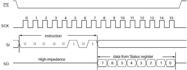
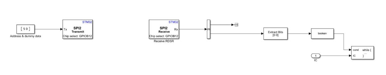
Poll the Write-In-Process (WIP) bit in the Read Status Register (RDSR), which is at address 0x05.
To poll the WIP bit:
Drive CS line low → Send
0x05(RDSR) → Send a dummy byte (0x00) to read the 8-bit register value.Check bit 0 (WIP). A value of 1, indicates Busy (the write is in progress). A value of 0, indicates Ready (the write is complete).
To read from the EEPROM, initiate this sequence of operations:
Drive CS line low.
Send
0x03(READ).Send 16-bit address (MSB then LSB).
Send dummy bytes to clock out data.
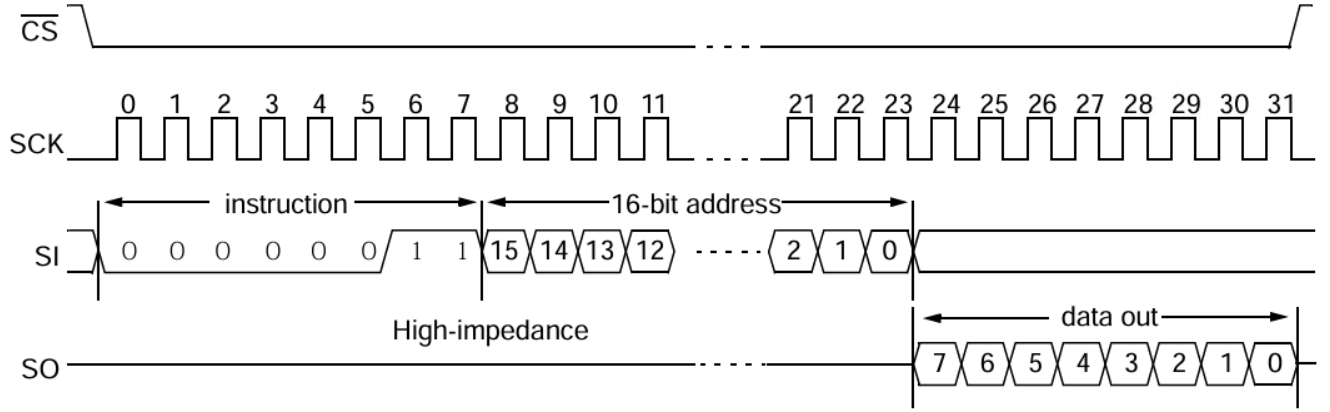
The address pointer automatically increments, allowing the entire array to be read in a single sequence,
Set Up Hardware Connections
Hardware connections depend on whether you use the EEPROM in your application.
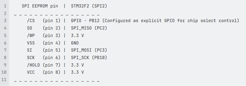
In this example, the STM32 Nucleo F207ZG board (acting as SPI controller) connects to a 25AA080 SPI EEPROM chip using SPI2.
Configure Microcontroller SPI Peripheral
Configure the microcontroller SPI peripheral with the following settings.
Parameter | Description | Where and How to Configure Parameter |
|---|---|---|
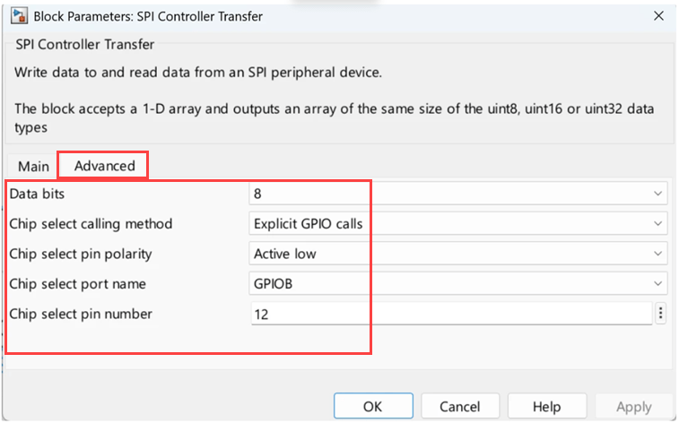
Data size | Set to 8-bit as specified in the Microchip 25XX080 8K SPI Bus Serial EEPROM datasheet | SPI block mask > Advanced Tab > Data bits |
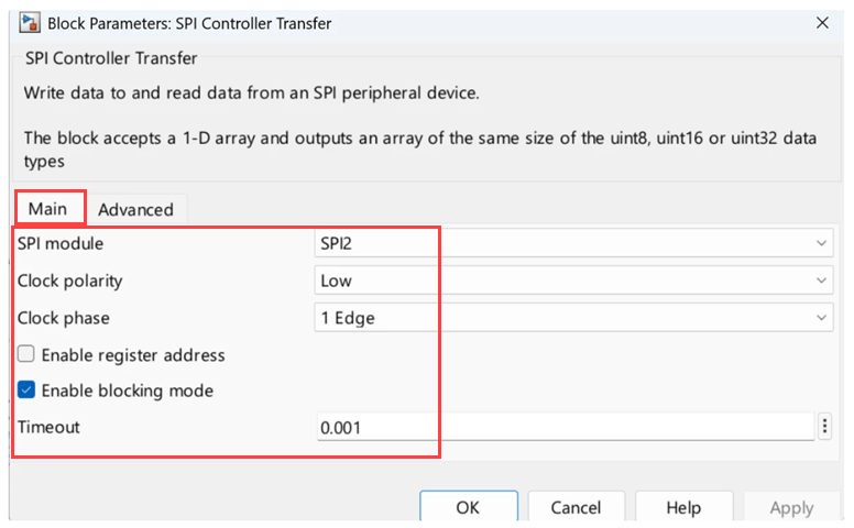
Clock polarity (CPOL)/ Clock phase (CPHA) | Data is sampled on the first rising edge of SCK. This implies that if Clock is Idle low, data is sampled at the first (rising) edge. If Clock is Idle high, data is sampled at the second (rising) edge. This resembles the following 2-clock polarity and clock phase configuration. CPOL=0 (Low), CPHA=0 (1 Edge) CPOL=1 (High), CPHA=1 (2 Edge) | SPI block mask > Basic Tab > Clock polarity & Clock phase |
Chip select | Use the GPIO pin for controlling CS. In this example we are using GPIO Port B (PB12). | In STM32CubeMX, set Hardware NSS Signal to SPI block mask > Advanced Tab > Set Chip select calling method to Set Chip select pin polarity to Set Chip select port name to Set Chip select pin number to |
Bit order | Most significant bit (MSB) first. | In STM32CubeMX, set First Bit to |
Clock frequency | Maximum 1 MHz for 25AA080 | In STM32CubeMX, set SPI Prescaler to a value which sets clock frequency to 1MHz |
For more information about the supported configuration, see the Microchip 25XX080 8K SPI Bus Serial EEPROM datasheet
Configure SPI2 Module
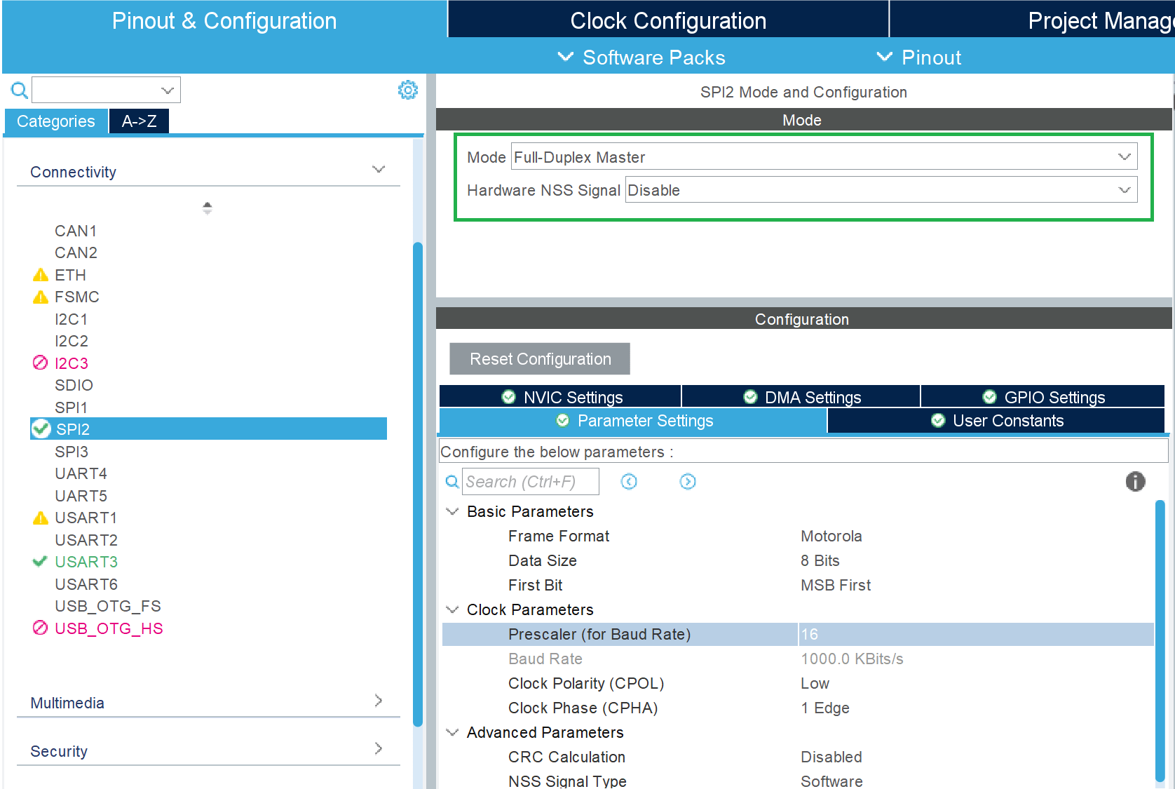
In STM32CubeMX, configure the SPI2 module as controller. STM32CubeMX saves the configuration in the IOC file.
1. On the Pinout & Configuration tab under Categories, select SPI2.
2. Under SPI2 Mode and Configuration:
Set Mode to
Full-Duplex Master. SPI2 serves as controller.Set Hardware NSS Signal to
Disable. This prevents the SPI bus from controlling the CS line. Instead, use the GPIO pin (PB12) for the CS line.
3. On the Parameter Settings tab:
Set Frame Format to
Motorola(derived from the timing diagram of CS and Clock).Set First Bit to
MSB First.Set Prescaler (for Baud Rate) based on the SPI clock frequency. Specify a baud rate that is within maximum support clock frequency of the EEPROM (1 MHz).
Note: The Data Size, Clock Polarity (CPOL), and Clock Phase (CPHA) parameters configured in the SPI block parameters override the corresponding settings in the STM32CubeMX .ioc file. Ensure that these block-level settings match the target SPI device requirements, as they determine the actual SPI behavior during code execution.
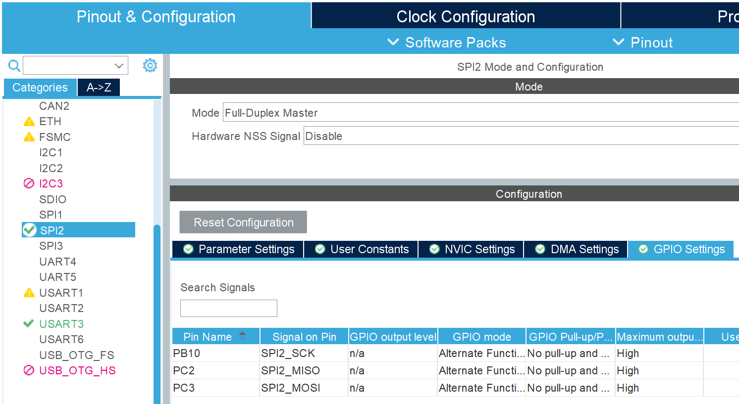
4. On the GPIO Settings tab, configure the SPI pins as this figure shows. GPIO Port-B pin-12 (PB12) is configure as GPIO output to control the chip select line.
Read and Write EEPROM Data Using SPI Controller Transfer Block
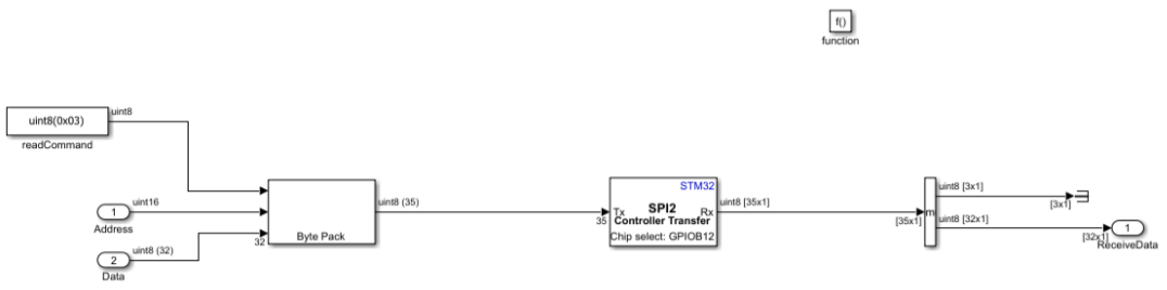
This example shows how to configure and use the SPI Controller Transfer block to perform simultaneous transmit and receive operations with an SPI EEPROM (25AA080) on STM32 processor-based boards. The block manages transmit/receive data, controls the chip select signal, and ensures equal amounts of transmitted and received data.
The SPI Controller Transfer block is best suited when you need to:
Perform full-duplex SPI communication (transmit and receive simultaneously)
Control chip select timing automatically
Work with fixed-length data vectors
Model Overview
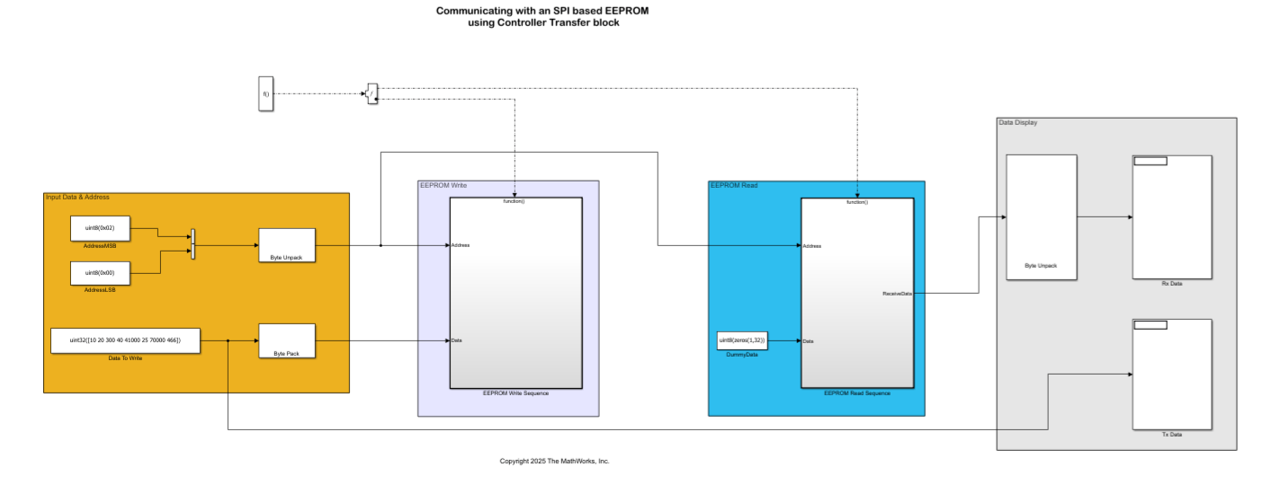
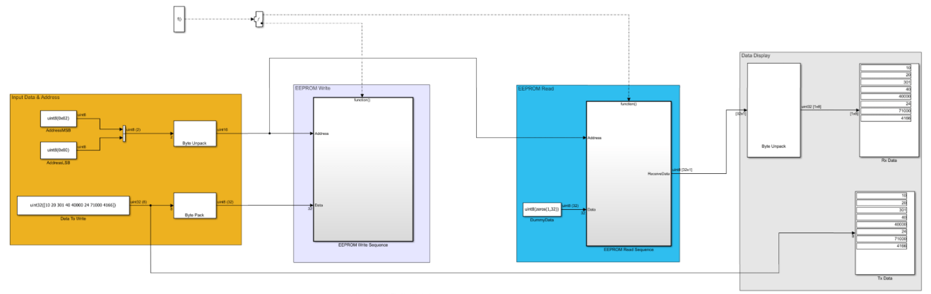
The example model spiEEPROMWithControllerTransferBlock.slx writes 32 bytes (eight packed uint32 values) to EEPROM address 0x0200 and reads back the same location to verify successful communication. It supports page-wise writes (16-byte pages).
The model contains two main subsystems:
EEPROM Write - Writes 32 bytes using two 16-byte page operations.
EEPROM Read - Reads back 32 bytes from address 0x0200.
Block Configuration
Open the SPI Controller Transfer block from the spiEEPROMWithControllerTransferBlock.slx example model. Configure the SPI module as shown below (SPI2 in this example):
EEPROM Write Subsystem
EEPROM Write subsystem writes 32 bytes to address 0x0200 in two 16-byte page operations.
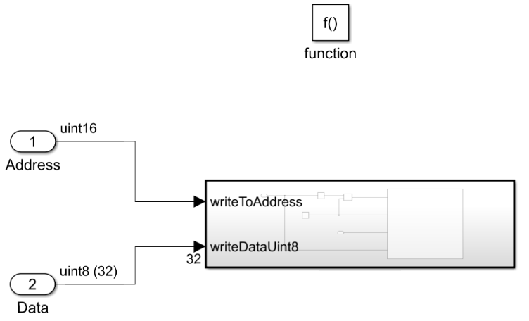
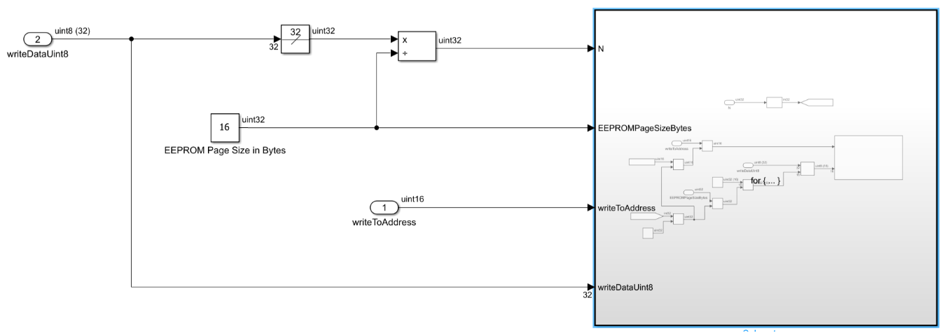
Key steps and rationale
Loop counter (N) — Divide total data width (32 bytes) by page size (16) → N = 2. This determines the number of page-write cycles required.
writeToAddress — Start address (uint16). Increment by 16 after each page using an Add block with offset 0x0010. Page addressing requires 16-byte alignment.
writeDataUint8 — Select 16 bytes per iteration using a Data Selector block. First iteration: bytes 1–16; second: bytes 17–32.
Page addressing logic - Byte Pack/Unpack blocks process LSB first, while EEPROM expects MSB first. To move to the next page correctly, add offset 0x1000 to the upper byte of the address.
This table shows an example with a step-by-step trace of what happens to the address bytes 0x02 and 0x00 (start address 0x0200).
Step | Operation | Value (Hex) | Explanation |
|---|---|---|---|
1 | Input | Byte 1: Byte 2: | Target address |
2 | Byte Unpack |
| The Byte Unpack block reads the first byte ( |
3 | Add Offset |
| Add |
4 | Byte Pack | Byte 1: Byte 2: | The Byte Pack block splits |
5 | SPI Transmit |
| Send these bytes to the EEPROM. |
6 | Hardware View | Address: | The EEPROM receives |
Write sequence steps
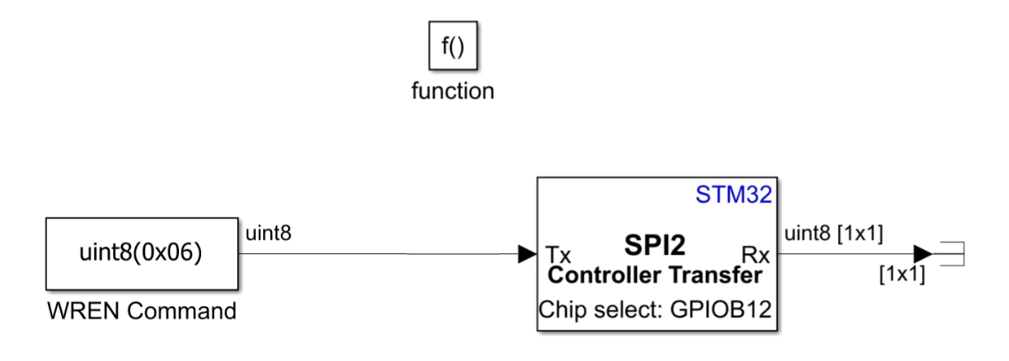
1. Send WREN (0x06) to enable the write latch.
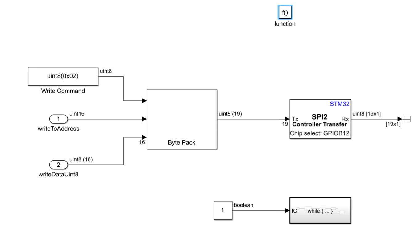
2. Construct write instruction: WREN (0x02) + 16-bit address + 16-byte data.
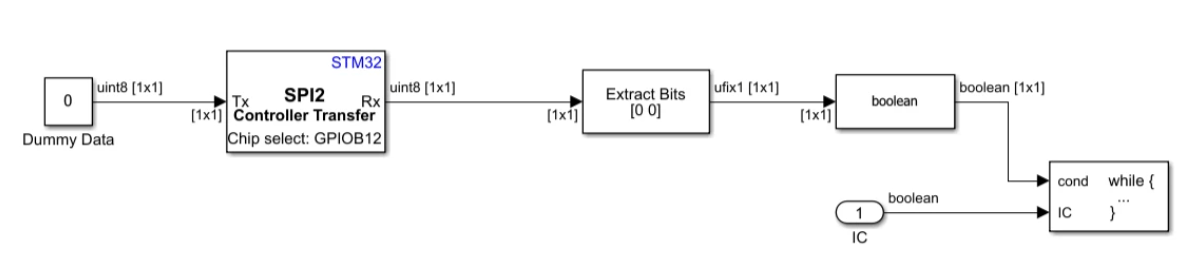
3. Poll RDSR register (0x05) using dummy read to check WIP bit = 0 (write complete).
4. The SPI2 Controller Transfer block is configured with the Register address parameter set to 0x05.This setting configures the RDSR register (0x05) such that it sends 1-byte dummy data to get the register value.
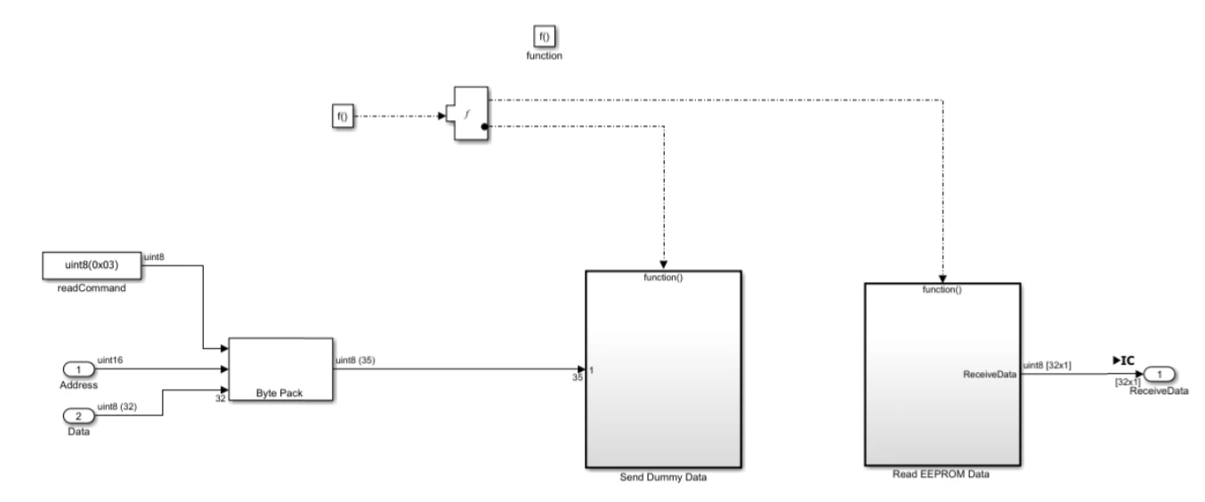
EEPROM Read Subsystem
EEPROM Read subsystem reads back 32 bytes from address 0x0200 after the write completes.
Key steps and rationale
Pack and transmit:
1-byte read command (0x03)
16-bit start address (0x0200)
32-byte dummy data (to keep clock and chip select active)
Total: 35 bytes transmitted.
Receive 35 bytes:
First 3 bytes (instruction + address) are discarded (not valid data)
Next 32 bytes contain the written data
Unpack the 32 bytes back into eight uint32 values to verify against the original write data.
Read and Write EEPROM Data Using SPI Transmit and Receive Blocks
This example shows how to use the SPI Transmit and SPI Receive blocks to read and write data to an SPI EEPROM (25AA080) on STM32 processor-based boards when transmit and receive operations occur at different rates or require independent control. The blocks allow separate management of chip select timing and data length, with buffered interrupt mode handling transfers larger than the SPI FIFO depth.
Use SPI Transmit and SPI Receive blocks when you need:
Independent transmit and receive operations
Different data rates or lengths for transmit vs. receive
Manual control over chip select timing
Model Overview
The example model spiEEPROMWithReceiveTransmitBlock.slx writes 32 bytes to EEPROM address 0x0200 and reads back the same location to verify successful communication. It uses separate subsystems for write enable, data transmit, write completion polling, and read operations.
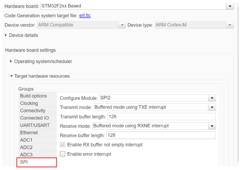
SPI Module Setup
Open Configuration Parameters (Ctrl+E).
In Hardware Implementation, select your STM32 board.
Configure the SPI module as follows (SPI2 in this example)
Transmit mode set to
Buffered mode using TXE interruptReceive mode set to
Buffered mode using RNXE interrupt
You do not need to add a Hardware Interrupt block to manage SPI interrupts. The SPI blocks handle interrupts internally to move transmit and receive data between the peripheral and a software buffer.
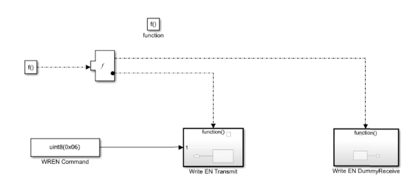
EEPROM Write Subsystem
The write operation uses three function-call subsystems: Write Enable, Write Data, and Wait for Write Cycle.
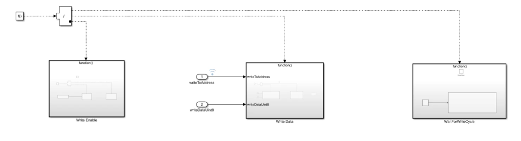
Write Enable
Use SPI Transmit block to send Write Enable command (0x06).
Follow immediately with SPI Receive block configured for 1-byte dummy receive.
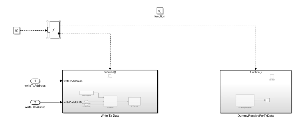
Write Data
Pack Write command (0x02) + 16-bit address + 32-byte data into a 35-byte vector.
Send using SPI Transmit block.
Follow with SPI Receive block configured for 35-byte dummy receive to keep clock active until all data is transmitted.
Wait for Write Cycle
Transmit address and dummy data to poll RDSR register (0x05). Check WIP bit = 0 to confirm write completion before proceeding.
EEPROM Read Subsystem
The read operation transmits and receives 35 bytes:
Pack read command (0x03) + 16-bit start address + 32-byte dummy data.
Transmit using SPI Transmit block.
Receive using SPI Receive block configured for 35 bytes.
Discard first 3 bytes (instruction + address).
Unpack remaining 32 bytes to verify against written data.