PCBWriter
R2026bCreate PCB board definitions from 2-D antenna designs
Description
Use the PCBWriter object to create a printed circuit board
(PCB) design files based on multilayer 2-D antenna design. A set of manufacturing files
known as Gerber files describes a PCB antennas. A Gerber file uses an ASCII vector
format for 2-D binary images.
Creation
Syntax
Description
b = PCBWriter(pcbstackobject)PCBWriter object that generates Gerber-format
PCB design files based on a 2-D antenna design geometry using PCB
stack.
b = PCBWriter(pcbstackobject,rfconnector)rfconnector
type.
b = PCBWriter(pcbstackobject,writer)writer.
b = PCBWriter(pcbstackobject,rfconnector,writer)
Input Arguments
Output Arguments
Properties
Object Functions
gerberWrite | Generate Gerber files |
openFolder | Open folder containing generated Gerber files in files browser |
sendTo | Export generated Gerber Files to service provider |
Examples
Create a coplanar inverted-F antenna.
fco = invertedFcoplanar(Height=14e-3,GroundPlaneLength=100e-3,...
    GroundPlaneWidth=100e-3);
Create a pcbStack object.
p = pcbStack(fco);
figure
show(p)
title("Inverted-F PCB Antenna")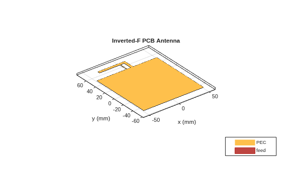
Generate a Gerber format design file using PCB Writer.
PW = PCBWriter(p)
PW =
  PCBWriter with properties:

                        Design: [1×1 struct]
                        Writer: [1×1 Gerber.Writer]
                     Connector: []
           UseDefaultConnector: 1
    ComponentBoundaryLineWidth: 8
         ComponentNameFontSize: []
            DesignInfoFontSize: []
                          Font: 'Arial'
                     PCBMargin: 5.0000e-04
                    Soldermask: 'both'
                   Solderpaste: 1
               EnableSignature: 1
          EnableConnectorLabel: 1

   See info for details
Create a coplanar inverted-F antenna.
fco = invertedFcoplanar(Height=14e-3,GroundPlaneLength=100e-3,...
    GroundPlaneWidth=100e-3);
Create a pcbStack object.
p = pcbStack(fco);
figure
show(p)
title("Inverted-F PCB Antenna")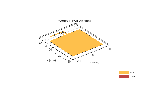
Create an SMA_Cinch connector using the PCBConnectors object.
c = PCBConnectors.SMA_Cinch
c =
  SMA_Cinch with properties:

                    Type: 'SMA'
                     Mfg: 'Cinch'
                    Part: '142-0711-202'
              Annotation: 'SMA'
               Impedance: 50
               Datasheet: 'https://belfuse.com/resources/Johnson/drawings/dr-142-0711-202.pdf'
                Purchase: 'https://www.digikey.com/product-detail/en/cinch-connectivity-solutions-johnson/142-0711-202/J10154TR-ND/3587681'
               TotalSize: [0.0071 0.0071]
           GroundPadSize: [0.0024 0.0024]
       SignalPadDiameter: 0.0017
         PinHoleDiameter: 0.0013
           IsolationRing: 0.0041
    VerticalGroundStrips: 1

   Cinch 142-0711-202 (Example Purchase)
Create a PCB design file for the antenna with the connector.
PW = PCBWriter(p,c)
PW =
  PCBWriter with properties:

                        Design: [1×1 struct]
                        Writer: [1×1 Gerber.Writer]
                     Connector: [1×1 PCBConnectors.SMA_Cinch]
           UseDefaultConnector: 0
    ComponentBoundaryLineWidth: 8
         ComponentNameFontSize: []
            DesignInfoFontSize: []
                          Font: 'Arial'
                     PCBMargin: 5.0000e-04
                    Soldermask: 'both'
                   Solderpaste: 1
               EnableSignature: 1
          EnableConnectorLabel: 1

   See info for details
Create a coplanar inverted-F antenna.
fco = invertedFcoplanar(Height=14e-3,GroundPlaneLength=100e-3,...
    GroundPlaneWidth=100e-3);
Create a pcbStack object.
p = pcbStack(fco);
figure
show(p)
title("Inverted-F PCB Antenna")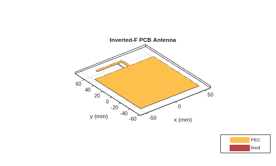
Use an Advanced Circuits Writer as a PCB manufacturing service.
s = PCBServices.AdvancedCircuitsWriter
s =
  AdvancedCircuitsWriter with properties:

               BoardProfileFile: 'legend'
          BoardProfileLineWidth: 1
                 CoordPrecision: [2 6]
                     CoordUnits: 'in'
              CreateArchiveFile: 1
                 DefaultViaDiam: 3.0000e-04
             DrawArcsUsingLines: 0
                 ExtensionLevel: 1
                       Filename: 'untitled'
                          Files: {}
         IncludeRootFolderInZip: 0
                   PostWriteFcn: @(obj)sendTo(obj)
    SameExtensionForGerberFiles: 0
                    UseExcellon: 1
Create an antenna PCB design file using the above service.
PW = PCBWriter(p,s)
PW =
  PCBWriter with properties:

                        Design: [1×1 struct]
                        Writer: [1×1 PCBServices.AdvancedCircuitsWriter]
                     Connector: []
           UseDefaultConnector: 1
    ComponentBoundaryLineWidth: 8
         ComponentNameFontSize: []
            DesignInfoFontSize: []
                          Font: 'Arial'
                     PCBMargin: 5.0000e-04
                    Soldermask: 'both'
                   Solderpaste: 1
               EnableSignature: 1
          EnableConnectorLabel: 1

   See info for details
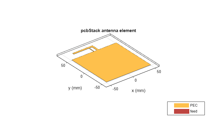
Create a coplanar inverted-F antenna.
fco = invertedFcoplanar(Height=14e-3,GroundPlaneLength=100e-3,...
    GroundPlaneWidth=100e-3);
Use this antenna to create a PCB stack object.
p = pcbStack(fco);
figure
show(p)
Use the GerbLookWriter to generate the Gerber files for the PCB.
s = PCBServices.GerbLookWriter;
Create an antenna design file using PCBWriter.
PW = PCBWriter(p,s);
Use the gerberWrite method to create Gerber files from the antenna design files.
gerberWrite(PW)
Generated File: 'C:\Users\user\OneDrive - MathWorks\Documents\MATLAB\ExampleManager\user.Bdoc.DocWork0\antenna-ex14839356\untitled.zip'
'(name is available in system cut-buffer)

13 files in PCB stack
   Size Lines File
     1k    64 untitled.gtl (Copper,L1,Top,Signal)
   239b    19 untitled.gts (Soldermask,Top)
   369b    29 untitled.gbs (Soldermask,Bot)
   285b    18 untitled.gbl (Copper,L2,Bot)
   308b    27 untitled.gtp (Paste,Top)
   215b    19 untitled.gbp (Paste,Bot)
   103b     6 untitled.txt (ExcellonPlated,1,2)
   207k 10349 untitled.gto (Legend,Top)
   118k  6204 untitled.gbo (Legend,Bot)
     1k    38 untitled.gpi (PhotoplotterInfo,Info)
     1k    36 untitled.dri (DrillStationInfo,Info)
   239b    17 untitled.ipc (IPCD356A,Info)
              untitled.gml (Profile,NP)
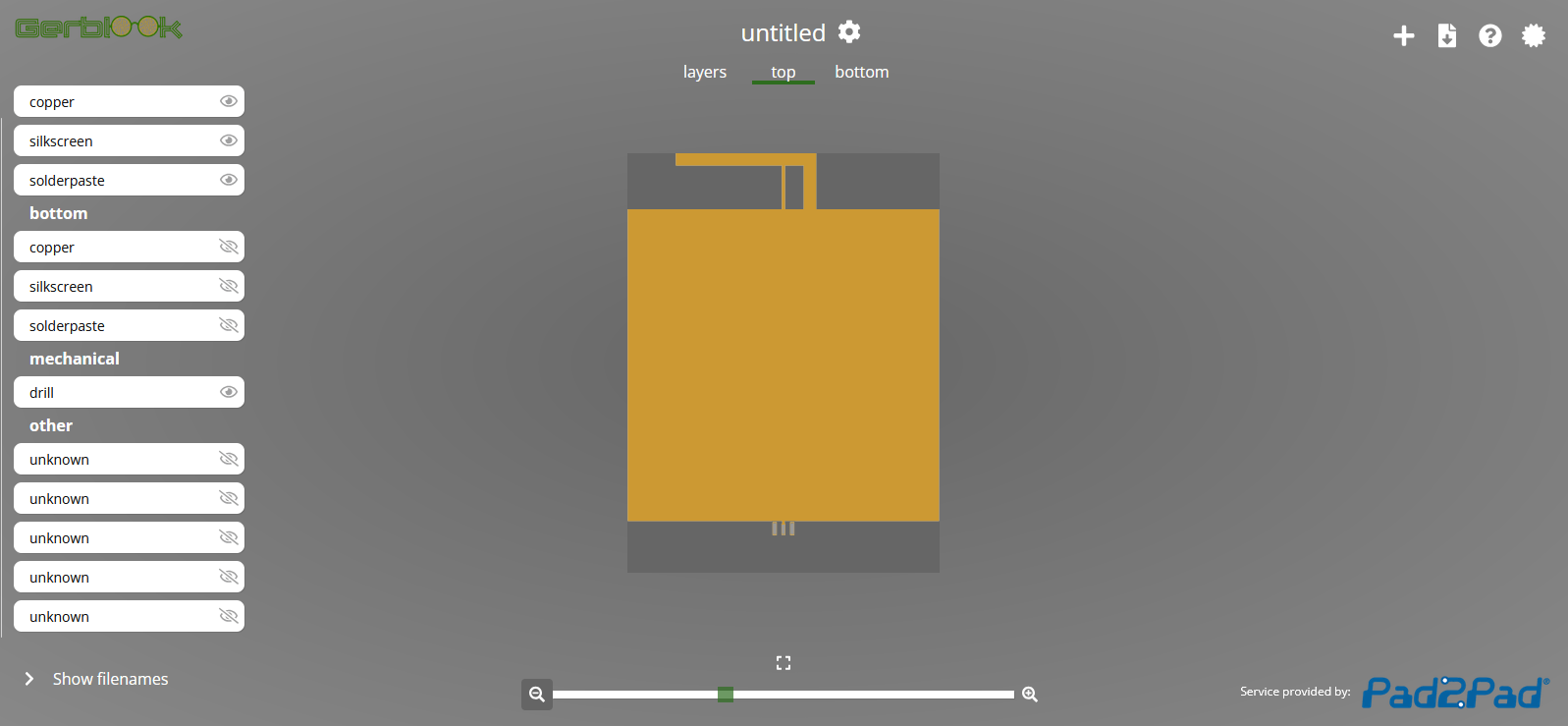
The location of the folder and the GerbLook viewer website opens automatically.
To view the board, drag and drop the files.