Design, Analysis, and Prototyping of Microstrip-Fed Wide-Slot Antenna
This example shows how to model a microstrip-fed printed wide slot antenna with FR4 substrate, analyze it and finally enables its prototyping by generating Gerber files. The design is intended for operation in the L-band and has a bandwidth of about 17% over the band 1.6 - 1.8 GHz.
Define Design Parameters
Define the design parameters of the antenna as provided in [1].
pcbThickness = 0.8e-3;
pcbMaterial = "FR4";
pcbEpsilonR = 4.4;
pcbTraceWidth = 1.5e-3;
gndLength = 110e-3;
gndWidth = 110e-3;
slotLength = 53.7e-3;
slotWidth = 53.7e-3;
offsetTraceLength = 28e-3;
pcbTraceLength = (gndWidth/2 - slotWidth/2) + offsetTraceLength;
Create Layer Shapes
Using the design parameters, create the basic shape primitives. The antenna has two metal layers on either side of a single-layer PCB. The first metal layer is the microstrip feedline and the second layer of metal is the ground plane with a wide slot cut out from it. After defining the shapes, use Boolean subtraction to create the slot in the ground plane.
feed = antenna.Rectangle(Length=pcbTraceWidth,Width=pcbTraceLength,...
    Center=[0, -gndWidth/2+pcbTraceLength/2],...
    NumPoints=[2 40 2 40]);
gnd = antenna.Rectangle(Length=gndLength,Width=gndWidth);
gndslot = antenna.Rectangle(Length=slotLength,Width=slotWidth);
gndPlane = gnd - gndslot;
figure
show(gndPlane)

Create Stack
Create the PCB stack by defining the dielectric material and arranging the layers in a top-down description starting with the top-most layer of metal. Define a feed location and the feed diameter as well. This antenna has the microstrip feedline brought out to the edge of the board.
d = dielectric(pcbMaterial);
d.EpsilonR = pcbEpsilonR;
d.Thickness = pcbThickness;
p = pcbStack;
p.Name = "Strip-fed slot";
p.BoardShape = gnd;
p.BoardThickness = pcbThickness;
p.Layers = {feed,d,gndPlane};
p.FeedLocations = [0,-gndWidth/2,1,3];
p.FeedDiameter = pcbTraceWidth/2;
figure
show(p)
Compute S-parameters
The antenna reflection coefficient reveals how well it responds to stimulus at any particular frequency. Typically, dB is considered to be good from an impedance matching perspective. The reference impedance here is the default of 50-ohms.
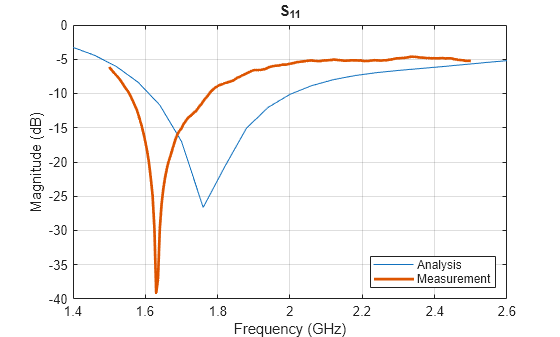
fmin = 1.4e9;
fmax = 2.6e9;
Z0 = 50;
N = 21;
freq = linspace(fmin,fmax,N);
s = sparameters(p,freq,Z0);
s11Fig = figure;
rfplot(s,1,1)

The plot of the reveals a good match to 50 within the band 1.6 - 1.85 GHz.
Generate and View Gerber Files
Gerber files are a commonly used format to export the geometry information of a PCB. To generate these files, two additional pieces of information are required apart from the PCB itself. The first is the type of connector to be used and the second is the PCB manufacturing service/viewer service. The type of RF connector determines the pad layouts on the PCB. The Antenna Toolbox™ provides a catalog of PCB services and RF connectors. The PCB services catalog supports configuring the Gerber file generation process for manufacturing as well as for online viewer-only.
The collection of Gerber files that describe a Printed Circuit Board (PCB) have each a different role. Each file describes a specific aspect of the PCB design. As an example, on the PCB there are metal regions corresponding to the signal and ground that are filled with Copper. This information is captured in the .gtl and .gbl files. Information about the solder mask, which is applied to protect and insulate the metal regions, is captured in the .gts and .gbs files. Design information is encoded into the silkscreen layer designated by .gto and .gbo files. To understand the generation process for these files use a PCB manufacturing service with an online viewer to render the design.
Online Gerber viewer
Use the MayhewWriter to configure the Gerber file generation process for the Mayhewlabs free online 3D Gerber viewer. Select an SMA edge connector from the catalog and modify it for this particular design. Use the PCB antenna model, the service and the RF connector to create a PCBWriter.
W = PCBServices.MayhewWriter;
W.Filename = 'Microstrip-fed slot patch-MH';
C = SMAEdge_SamtecCustom;
C.EdgeLocation = "south";
C.ExtendBoardProfile = false;
Am = PCBWriter(p,W,C);
Generate Gerber files
Use the gerberWrite function to generate the Gerber files.
gerberWrite(Am)
The files are generated and placed in a zipped folder with the same name as assigned in the Filename property of the specified PCB service. The location of the folder is the current working directory. The files in the folder are shown in the image below.

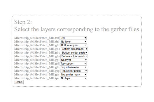
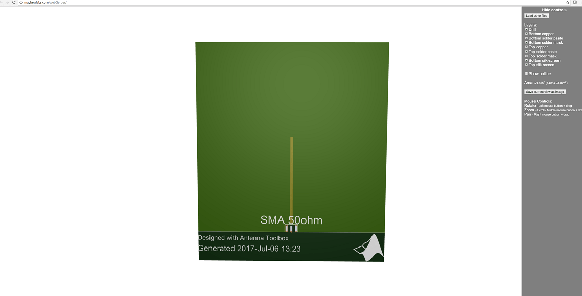
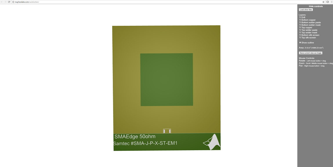
In addition to this, if the internet access is available, a browser window opens up for the Mayhewlabs free 3D online Gerber viewer. Select and drag all the generated files into the browser window. The files and their purpose are organized as shown below. When ready click on Done.
The PCB design described by the set of Gerber files is now rendered in the browser window. Use the mouse to orient and position the design. The menus on the right of the screen enables selective viewing of different parts of the Gerber file such as the soldermask, copper layers and silkscreen.
PCB Service for Manufacturing
Use the SeeedWriter to configure the Gerber file generation process for the Seeed Fusion PCB manufacturing services. Regenerate the PCBWriter with the new service.
W = PCBServices.SeeedWriter;
W.Filename = 'Microstrip-fed slot patch-SS';
As = PCBWriter(p,W,C);
Use the gerberWrite function to generate the Gerber files.
gerberWrite(As)
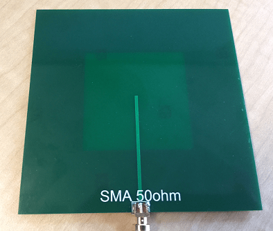
Manufactured Antenna and Measurements
Submit the order on the Seeed Fusion website together with the generated Gerber files. The manufactured antenna is mailed out in a few weeks.
The reflection coefficient of the prototype antenna was measured in the Antenna Lab at Worcester Polytechnic Institute (WPI). The results are plotted as shown below.
s11_1 = readmatrix("TRACE01.CSV");
freq_trace = s11_1(:,1)./1e9;
s11Data = s11_1(:,2);
figure(s11Fig);
hold on
plot(freq_trace,s11Data,LineWidth=2);
legend("Analysis","Measurement",Location="SouthEast")
title("S_1_1");
hold off
Conclusion
The agreement between the analyzed and measured results is reasonable with approximately 4% absolute error in the minimum.
Reference
[1] Jia-Yi Sze and Kin-Lu Wong, "Bandwidth enhancement of a microstrip-line-fed printed wide-slot antenna," in IEEE Transactions on Antennas and Propagation, vol. 49, no. 7, pp. 1020-1024, Jul 2001.