Guidelines for Using Assignment Blocks to Write Elements in Vectors, Matrices, and 3-D Arrays
Follow these guidelines when writing input signals to an element in a vector, matrix, or 3-D array signal.
Each guideline has a severity level that indicates the level of compliance requirements. To learn more, see HDL Modeling Guidelines Severity Levels.
Guideline ID
2.3.4
Severity
Recommended
Description
You can use the Assignment block to write input signals to an element in a vector, matrix, or 3-D array signal. For HDL code generation, use these block parameter settings:
Number of output dimensions: Set this parameter to
1when the output is a vector,2for a 2-D array, or3for a 3-D array.Index mode: Use zero-based indexing so that the generated code matches the model.
Initialize output (Y): Set this parameter to
Initialize using input port <Y0>, which initializes the output with the signal at the input port Y0. You cannot use theSpecify size for each dimension in tablesetting for HDL code generation. To enable this parameter, set Index Option toIndex vector (port)orStarting index (port)for one or more dimensions.Index option:
When using an Assignment block that has a variable index for an application such as register bank usage, choose a port-related setting, such as
Index Vector
                                            (port)
. For a fixed index, select from dialog-related settings, such asIndex vector (dialog).When assigning individual values to multiple elements of the output port Y, use an input signal with the same size as the elements specified by setting of the Index option parameter.
When assigning the same value to multiple elements, use a scalar input signal regardless the setting of the Index option parameter.
Model a Register Bank by Using Assignment Block
This example shows how to model a register bank by using the Assignment block.
The hdlcoder_assignment_vector model contains an Assignment block that has variable index, a Delay block, and a Reshape block. To model as a register bank, the model employs a feedback loop from the output of the Reshape block to the input signal, Y0, of the Assignment block Y0. By specifying a scalar value to the input signal U as the register value and limiting the index from the port to one write address, the model behaves as a register bank. When you specify multiple elements to the input Idx1, the model simultaneously rewrites the elements in the output signals.
load_system("hdlcoder_assignment_Vector")
open_system('hdlcoder_assignment_Vector/DUT_Vector')
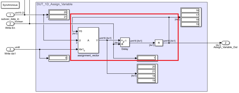
When the column vector output [16;17;18;19] from the Delay block is input as the Y0 value, a column vector [20;21] with two elements is input to the write input signal U. Because the start index of Idx1 is 0, the input signal U overwrites the 0th to 1st element of Y0, and the output signal Y becomes the column vector [20;21;18;19]. The Delay block outputs signal Y when the Write En signal is valid, or otherwise holds previous value.
Generate the HDL code for DUT_Vector subsystem.
makehdl('hdlcoder_assignment_Vector/DUT_Vector')### Working on the model hdlcoder_assignment_Vector ### Generating HDL for hdlcoder_assignment_Vector/DUT_Vector ### Using the config set for model hdlcoder_assignment_Vector for HDL code generation parameters. ### Running HDL checks on the model 'hdlcoder_assignment_Vector'. ### Begin compilation of the model 'hdlcoder_assignment_Vector'... ### Working on the model 'hdlcoder_assignment_Vector'... ### Working on... GenerateModel ### Begin model generation 'gm_hdlcoder_assignment_Vector'... ### Copying DUT to the generated model.... ### Model generation complete. ### Generated model saved at hdlsrc\hdlcoder_assignment_Vector\gm_hdlcoder_assignment_Vector.slx ### Begin Verilog Code Generation for 'hdlcoder_assignment_Vector'. ### Working on... Traceability ### Working on... HDLGenerateWebview ### Working on hdlcoder_assignment_Vector/DUT_Vector as hdlsrc\hdlcoder_assignment_Vector\DUT_Vector.v. ### Code Generation for 'hdlcoder_assignment_Vector' completed. ### Generating HTML files for code generation report at hdlcoder_assignment_Vector_codegen_rpt.html
Warning: Model Web view in code generation report requires Simulink Report Generator, which is not installed.
### Creating HDL Code Generation Check Report DUT_Vector_report.html
### HDL check for 'hdlcoder_assignment_Vector' complete with 0 errors, 0 warnings, and 0 messages.
### HDL code generation complete.
The hdlcoder_assignment_Matrix and hdlcoder_assignment_3D_Array models extend this register bank model for 2-D and 3-D.
open_system('hdlcoder_assignment_Matrix')
open_system('hdlcoder_assignment_3D_Array')