Use FPGA I/O to Communicate with FPGA on Zynq-Based Radio by Using MATLAB
This example shows how to prototype an FPGA design on a Xilinx® Zynq®-based radio and communicate with hardware by using MATLAB® as the host computer. In this example, you can deploy a waveform transmitter and receiver algorithm on hardware, and then transmit and receive the stream signals through the MATLAB® host.
In this example, you to interact with an FPGA design that is running on the hardware. Working with hardware helps you to rapidly prototype designs, verify functionality, tune key parameters, connect to real-world signals, collect data for analysis, and more.
This example highlights how to:
Generate simple algorithm that runs on hardware.
Generate HDL IP core and host interface script for your design.
Use host interface script to establish connection with the hardware.
Deploy bitstream and integrate HDL IP core on hardware.
Write input stream signal to your FPGA design.
Read output stream signal from your FPGA design for analysis.
Prerequisites
Install and configure these support packages and third-party tools.
HDL Coder™ Support Package for AMD® FPGA and SoC Devices
Xilinx Vivado® (version indicated in HDL Language Support and Supported Third-Party Tools and Hardware.
MathWorks® firmware image on the board’s SD card. See Guided Hardware Setup for AMD Boards.
Hardware Board Setup
After downloading MathWorks® firmware image to the SD card, follow these instructions to setup the hardware board:
Set the Jumper switch positions to [0,0,1,1,0] as shown in the image below.
Remove the SD card from the host computer and insert it into the ZC706 board.
Make the required connections between hardware board and development host computer.
Connect the antennas or loopback cable to Add-On card.
Plug the RF Add-On card into the LPC FMC connector.
Connect the power cable to the board.
Turn on the power button.
Once the board is powered ON, wait until LEDs light up, which indicates the radio is ready.

If you do not see the LED's light up as indicated, go back and verify whether the:
Jumper switch positions are in the correct position.
SD card has been properly inserted.
If the LED's do not light up after waiting for sometime, press PS-POR push button to reset and restart the board.
System Architecture
This figure shows the high-level architecture of the system in this example.The host computer communicates to the FPGA through the processing system on the System on Chip (SoC) board. The host computer can also tune parameters by writing to AXI4-Lite registers in the algorithm IP core.

The HDL IP core on the Zynq® programmable logic (PL) combines:
Waveform transmission from the FPGA RAM to the radio front end
Power signal computation of both the transmitted and received waveforms
Triggering logic
The Zynq® processing system (PS) performs these tasks:
Loading the waveform from the ARM processor to the FPGA RAM for transmission onto SDR
Receiving the computed power signals from the PL
Unlike the code generation and deployment on the PS, which happens while using software interface model, when you use the fpga() function in the MATLAB host, the IIO drivers in the PS transmit and receive the signals.
The waveform transmission and reception is trigger-based and the algorithm computes the power signals of the transmitted and received waveforms. Because the algorithm is trigger-based and deals with packetized data, the example uses AXI4-Stream interface instead of the I/Q stream to manage the data transmission between the ARM processor and the FPGA.
The HDL IP core has these port interfaces:
AXI4-Stream input ports for writing the waveform into FPGA RAM
AXI4-Stream output ports for reading the computed power of transmitted and received signals into the PS
AXI4-Lite input ports for real-time control and adjustment of the design
AXI DMA ports for data movement of the I/Q samples between the HDL IP core and the PS
The transmitter and receiver base-band ports for data movement of the I/Q samples between the HDL IP core and the AD936x IP
Open the Model
The hdlcoder_radio_loopback model is compatible with hardware generation. You can use this model to generate HDL code for the PL and generate a host interface script by using the HDL Workflow Advisor. Using the host interface script, you can connect to the design running on the hardware.
The HDL_DUT subsystem models the functionality to be implemented on the PL. The highlighted blocks outside the subsystem represent the control functionality to be implemented on the PS.
modelname = 'hdlcoder_radio_loopback';
load_system(modelname);
open_system(modelname);

The Tx and Rx subsystems model the transmitter and receiver logic of the PL algorithm, respectively.
currentSubSys = 'HDL_DUT';
open_system([modelname '/' currentSubSys]);
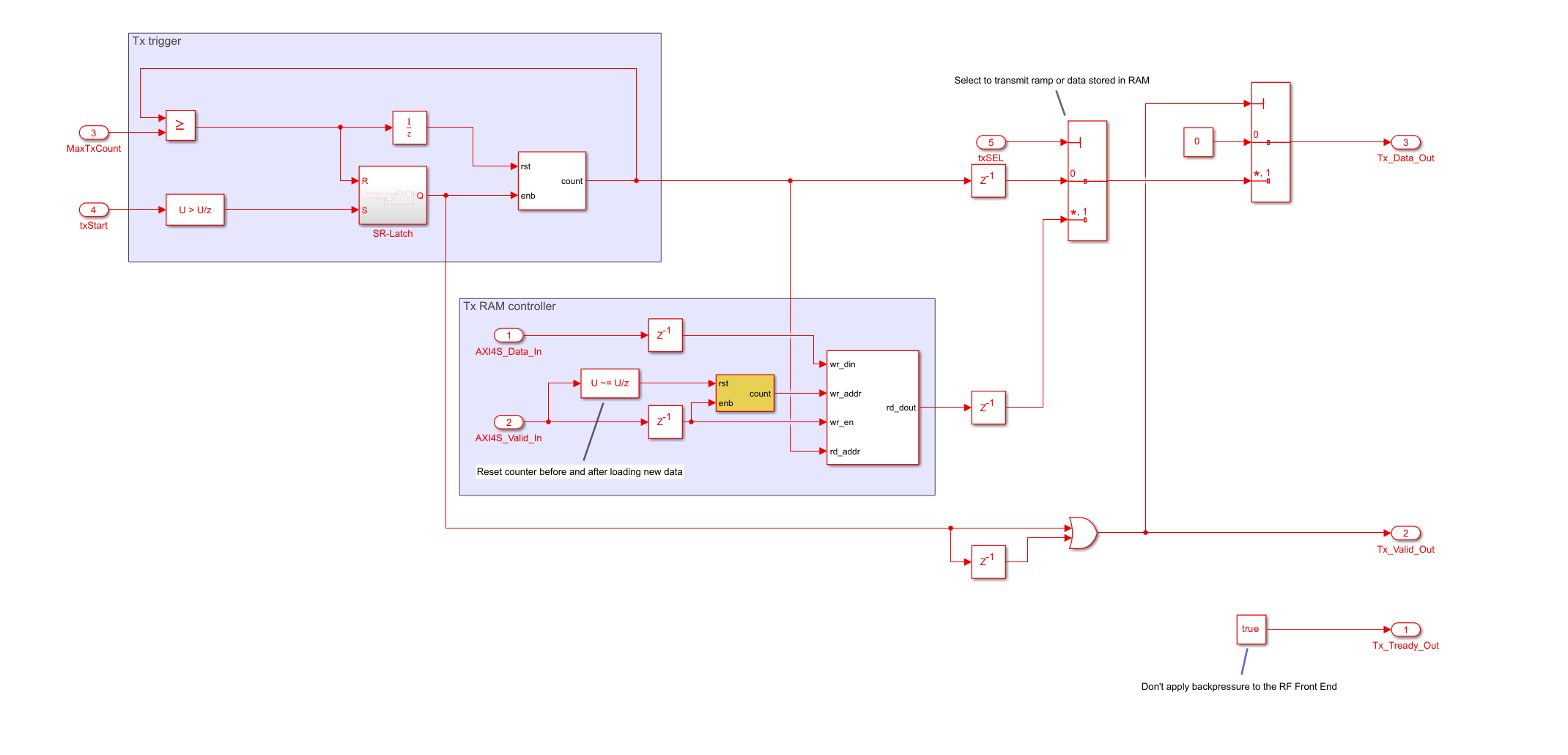
In the Tx subsystem, a valid input frame of AXI4-S data writes to the dual-port block RAM. The maxTxCount and txSel input ports control the transmission of the data in the Tx subsystem, and the txStart input port triggers the transmission of data.
currentSubSys = 'HDL_DUT/Tx';
open_system([modelname '/' currentSubSys]);

The Rx subsystem computes the power for both the transmitted and received signals as I/Q squared magnitude. To provide padding, the Valid Out Output port outputs a valid period that corresponds to 1.5 times the frame size of the transmitted signal. This padding accounts for the time taken for the transmitted waveform to appear at the receiver.
currentSubSys = 'HDL_DUT/Tx';
open_system([modelname '/' currentSubSys]);

The HDL_DUT subsystem has designated ports that model AXI4 data paths between the PS and PL.
The AXI4-Lite registers are:
maxTxCount, which defines the maximum number of transmit signal samples (up to 2047)txStart, which triggers a single transmission ofmaxTxCountsamples when set to truetxSel, which switches between transmitting data stored in the FPGA RAM to the PS or to the ramp signal
The AXI4-Stream interfaces are:
AXI4S_Data_In, which loads transmission data from the PS to the FPGA RAMAXI4S_Data_Out, which retrieves computed power of Tx and Rx signals to the PS
Simulate the Model
Simulate this model to confirm its operation. A chirp signal is defined in workspace variable inpSig. The Tx Data block reads the signal into the model and scales it for representation by the int16 fixed-point data type. The Write Tx Data block generates AXI4-Stream Data and Valid signals, which writes the signal samples to RAM in the HDL_DUT subsystem. The Max Tx Count, Tx Start and Tx Select blocks model the AXI4-Lite control registers.. The values of these blocks trigger a single transmission of the chirp signal, followed by a single transmission of the ramp signal for 2047 samples which loop back over the I/Q interfaces. This transmission triggers a receive at the same time which captures both the transmitted and received signal for a certain length and calculates the power of both signals before transferring them over the AXI4-Stream Data and Valid signals.
The image shows the power output of the Tx and Rx data frames in the Scope block.

After the simulation completes, you can start the process of generating the HDL IP Core, integrating the core with the SDR reference design, and generating the host interface script.
Generate the IP Core
First set up the Xilinx Vivado tool by using the hdlsetuptoolpath function. Use your own Xilinx Vivado installation path when executing the command.
>> hdlsetuptoolpath('ToolName','Xilinx Vivado','ToolPath',vivadopath);
Register the custom boards to MATLAB path for creating a Vivado project by entering these commands:
hdlcoder_amd_examples_root
addpath(fullfile(hdlcoder_amd_examples_root,'ZC706'))
addpath(fullfile(hdlcoder_amd_examples_root,'ipcore'))
Make sure that you have installed the HDL Coder Support Package for AMD FPGA and SoC Devices.
Right-click the HDL_DUT subsystem and select HDL Code > HDL Workflow Advisor.
1. In step 1.1, set Target workflow to IP Core Generation and Target platform to Xilinx Zynq ZC706 evaluation kit.

2. In step 1.2, set Reference design to Radio loopback with AXI4-Stream Interface. For this example, you can use the default reference design parameters.

3. In step 1.3, review the data in the Target platform interface table section. The Workflow Advisor automatically maps the DUT signals to the interface signals in the reference design.

4. In step 1.4, set the Target Frequency (MHz) parameter to the DUT synthesis frequency.. The DUT synthesis frequency depends on the baseband sampling rate of the system. In this example, the sample rate is 3.84 MHz, so a synthesis frequency of at least 4 MHz is sufficient.
5. Right-click step 2 and click Run to Selected Task to perform the design checks.
6. Right-click step 3 and click Run to Selected Task to generate the HDL code for the IP core.

Generate Host Interface Script
Next, you use the generated host interface script and modify it to:
Create a hardware object to establish a connection to your FPGA.
Deploy the bitstream on hardware.
Write input control signals and stream signals to the PS.
Read the output stream signals from the PS.
After you use the fpga function to read the stream signal from the PS to the MATLAB host, you unpack the data to visualize the behaviour of the design.
To generate a host computer interface to the IP core and deploy the design to the target hardware board:
1. In step 4.1, click Run This Task.. This task inserts the generated IP core for the FPGA algorithm into the reference design and creates the system shown in the system architecture diagram.
2. In step 4.2, select Generate host interface script and clear the Generate Simulink software interface model. Then, click Run this task.
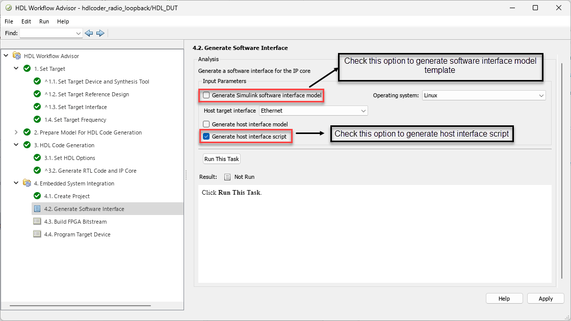
The HDL Workflow Advisor generates two MATLAB files in your current folder. You can use these files to prototype your generated IP core directly from MATLAB.

Currently, external mode is not supported to the Radio Loopback with AXI4-Stream Interface reference design. Hence, selecting Generate software interface model option may result in unexpected errors
Generate Bitstream
Step 4.3 generates a bitstream for the PL. You can execute this step in an external shell by selecting Run build process externally. This selection allows you to continue using MATLAB while building the FPGA image. Next, click Run This Task. After the HDL Workflow Advisor completes the product checks, it marks step 4.3 with a green check mark. You must wait until the external shell displays a successful bitstream build before continuing on to the next step.

When the bitstream is ready, you can load it on the hardware board by using the host interface script.
Interact with the FPGA Design from the Host Computer
Interact with the FPGA design by reading and writing data through MATLAB on the host computer.
Open the generated script file by entering:
open gs_hdlcoder_radio_loopback_interface.mUsing host interface script, you can:
Program the FPGA hardware with the generated bitstream and configure the processor with the device tree, which requires board IP address as well.
Create an
fpgahardware object, which represents a connection to the FPGA on your hardware board.Configure the
fpgaobject with the desired hardware interfaces and ports from your DUT algorithm.Read and write data to the DUT to exercise your algorithm on the hardware.
Release the hardware board from the current MATLAB session.

You can modify the interface script depending on the algorithm implemented in your Simulink model.
Open the generated setup function by entering:
open gs_hdlcoder_radio_loopback_setup.mThis function configures the fpga hardware object with the same ports and interfaces specified in task 1.3. Set Target Interface.
Under AXI4-Lite section, DUT input ports such as
maxTCount,txStart,andtxSelare mapped to AXI registers because the table in step 1.3 declared these ports as AXI4-Lite.Similarly, the DUT input port
AXI4S_Data_Inand DUT output portAXI4S_Data_Outare mapped to AXI4-Stream Read and AXI4-Stream Write, respectively.
 l
l
You can also modify the setup script depending on the algorithm you implement in your Simulink model. You can alter parameters, such as WriteFrameLength and ReadFrameLength, as shown in this example. In this setup script, the values for WriteFrameLength and ReadFrameLength have been adjusted from 1024 to 2048. However, you cannot change parameters like IOInterface because they have been defined to work as intended.
Configure the Software Defined Radio (SDR)
This example uses the System Object hdlcoder.sdr to configure the AD9361/AD9364 transmitter and receiver, respectively. The transmitter and receiver do not send data from the PS to the PL but configuring them initializes RF parameters and enables transmit and receive data paths. 
Before performing any write or read operations using host interface script, the configure the SDR. If not, the SDR can take erroneous values and exhibit unexpected behaviour.
Run Host Interface Script on the Target
Modify the generated host script as shown in this code. First, initialize all the variables in the script and then load the generated bitstream on the hardware board. The sel variable selects between the internally generated ramp signal and externally passing signal. After the bitstream loads, you can verify the SDR connection to hardware. This program device is a one time process and after successfully programming the device with bitsream, you can comment out the programFPGA and configuration of SDR section.
%% Variables Initialization

IPAddress = '192.168.3.2'; %Hardware board IP address
Fc = 2.4e9;    %Center Frequency
Fs = 3840000;  % Sampling Frequency
nsamp = 2048;  %Number of time samples
ntxSampleS = 2048;     %Number of transmit signal samples
txGain = -10;  %SDR transmitter gain
rxGain = 1;    %SDR receiver gain
FrameSize = 2048;
t = (0:nsamp)/Fs;

% sel - 0: To see internal signal present in LUT inside the Tx subsystem
% sel - 1: To see the externally passing signal from MATLAB host
sel = input('Enter 0 to see the internal ramp and 1 for externally passing signal:  ') %#ok<NOPTS>
sel =
1
hProcessor = xilinxsoc(IPAddress,'root','root');
programFPGA(hProcessor, "hdl_prj\vivado_ip_prj\vivado_prj.runs\impl_1\system_top.bit", "devicetree_fmcomms2_axis.dtb");
### Programming FPGA device on Xilinx Zynq ZC706 hardware board at 192.168.3.2...
### Copying FPGA programming files to SD card...
### Setting FPGA bitstream and devicetree for boot...
# Copying Bitstream system_top.bit to /mnt/hdlcoder_rd
# Set Bitstream to hdlcoder_rd/system_top.bit
# Copying Devicetree devicetree_fmcomms2_axis.dtb to /mnt/hdlcoder_rd
# Set Devicetree to hdlcoder_rd/devicetree_fmcomms2_axis.dtb
# Set up boot for Reference Design: ''
### Rebooting Xilinx Zynq ZC706 at 192.168.3.2...
### Reboot may take several seconds...
### Attempting to connect to the hardware board at 192.168.3.2...
### Connection successful
%% Create fpga object

hFPGA = fpga(hProcessor);
%% Configure SDR SDRTxRx = hdlcoder.sdr('AD936x', ... IPAddress = IPAddress,... CenterFrequency = Fc,... ChannelMapping = [1 2],... BasebandSampleRate = Fs,... TxGain = txGain,... RxGain = rxGain,... SamplesPerFrame = FrameSize); setup(SDRTxRx);
## Establishing connection to hardware. This process can take several seconds.
## Establishing connection to hardware. This process can take several seconds.
%% Setup fpga object
% This function configures the "fpga" object with the same interfaces as the generated IP core

gs_hdlcoder_radio_loopback_setup(hFPGA);
%% AXI4-Stream Read

%writePort(hFPGA, "AXI4S_Data_In",int32(1000*sin(2*pi*20e3*(0:2047)/Fs)));
writePort(hFPGA, "AXI4S_Data_In",int32(1000*chirp(t(1:2048),0,t(2048),Fs/20,[],90)));
%writePort(hFPGA, "AXI4S_Data_In",int32(1000*sawtooth(2*pi*20e3*(0:2047)/Fs)));
%% AXI4 Lite

if(sel == 0)
 writePort(hFPGA, "txSel", zeros([1 1]));
else
 writePort(hFPGA, "txSel", ones([1 1]));
end
 writePort(hFPGA, "maxTxCount", int16(ntxSampleS-1));
 writePort(hFPGA, "txStart", ones([1 1]));
%% AXI4-Stream Write

data_AXI4S_Data_Out = readPort(hFPGA, "AXI4S_Data_Out");
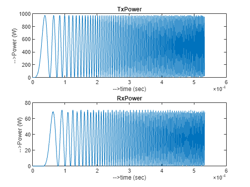
%% Data Unpacking

dataReceived = typecast(data_AXI4S_Data_Out,'int16');
rxPower = dataReceived(1:2:4096);
txPower = dataReceived(2:2:4096);
subplot(2,1,1)
%figure
plot(t(1:end-1),txPower)
title('TxPower');
xlabel('-->time (sec)')
ylabel('-->Power (W)')
subplot(2,1,2)
%figure
plot(t(1:end-1),rxPower)
title('RxPower');
xlabel('-->time (sec)')
ylabel('-->Power (W)')
release(hFPGA);
delete(hFPGA);
After the SDR configuration completes, the writePort function passes input stream signal and control signals and the data coming from the DUT output port AXI4S_Data_Out is read into data_AXI4S_Data_Out through readPort.
The data type of the AXI4S_Data_Out is int32. The MSB 16 bits contains the information pertaining to TxPower. LSB 16 bits contains the information of RxPower. Hence data unpacking is required to separate TxPower and RxPower.
Finally, the release command releases the fpga handle from the MATLAB session and the delete command deletes the variable completely from the MATLAB workspace.