Circuit Design Details Affect PLL Performance
This example shows how to use the circuit analysis tools from Mixed-Signal Blockset™ to evaluate the effects of loop filter circuit design details on the performance of a phase-locked loop.
Analog circuit imperfections such as circuit element limitations, element value variations, layout parasitics, and device noise can all measurably affect system-level performance. To release a system design for production, you need to evaluate the effects of these analog circuit design details to confirm that the manufactured system meets its performance requirements. For linear time-invariant analog circuits, the cktblock can help by directly solving the detailed circuit equations and packaging the solution in the form of behavioral blocks that will execute efficiently in a Simulink® model.
Open the model PllAnalogCircuitExample attached to this example.
model = "PllAnalogCircuitExample";
open_system(model);

The model defines an integer-N single modulus PLL using the basic building blocks from Mixed-Signal Blockset™. The loop filter for the PLL is circuit is defined using Simscape™ blocks and implemented using a behavioral model. For more information on the PLL model, see Phase Noise at PLL Output.
The PLL Testbench supplies a reference input signal for the PLL. This reference signal is modulated by a PRBS6 phase modulation that is used to measure the closed loop phase noise transfer function of the PLL. The input spectrum is evaluated by a spectrum estimator.
The output spectrum is measured both by the PLL Testbench and by a spectrum estimator like the one used to measure the input spectrum.
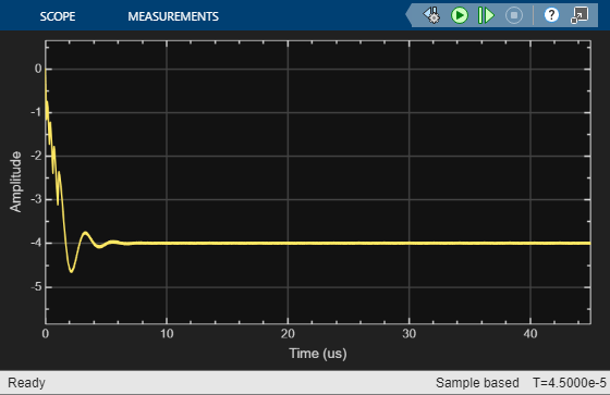
The model includes a scope to measure the PLL loop lock time.
Initial System Design
The chosen loop filter design is a third order passive loop filter, R2 = 1.33 kΩ, R3 = 17 kΩ, C1 = 13.1 pF, C2 = 144 pF, and C3 = 0.941 pF [1].

The other primary loop design parameters are:
Reference frequency:
30MHzPrescaler divider ratio:
70VCO sensitivity:
100MHz/VCharge pump output current:
1mA
The primary circuit impairments are:
VCO phase noise

Charge pump imbalance:
0.1mACharge pump leakage:
0.01mAReference PRBS6 modulation peak level:
-60dBc/Hz
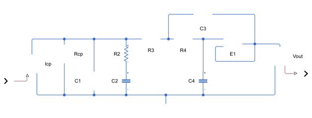
To create the loop filter block, start by creating or obtaining a Simscape™ schematic of the circuit. This example uses a third order passive loop filter defined in ThirdOrderPassiveLoopFilter.slx. This schematic includes the independent current source Icp to define a current input port and the voltage output port Vout.
schematic = "ThirdOrderPassiveLoopFilter";
open_system(schematic);

Use the cktconfig function to parse the circuit's configuration from the schematic.
cfg = cktconfig(schematic);
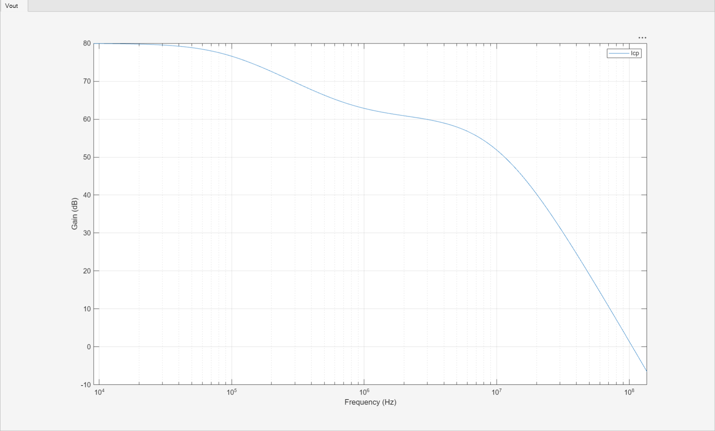
View the circuit's transfer function using cktzpk.
cktzpk(cfg,DisplayPlot=true);

Use cktblock to extract a behavioral model of the loop filter circuit from the circuit configuration object cfg and use that model in Simulink®. Create the block in PllAnalogCircuitExample.
block = "Loop Filter";
cktblock(cfg,model,CircuitDesignName=schematic,BlockName=block);
Connect the new Loop Filter block between the Charge Pump and VCO blocks.
set_param(model + "/" + block,Position=[730 226 900 284]);

In the configuration of this model, the charge pump impairments are activated. Therefore, the charge pump defines a fixed step discrete sample time to drive the loop filter. Enabling the impairments also provides the level of detail needed in the later stages of development, at the cost of increased simulation run time. If the charge pump impairments are disabled, then the loop filter can be configured to provide its own sample time. However, a lowpass resampler, such as that used in the Loop Filter block, is required to convert from the variable step discrete sample time of the charge pump without impairments to the fixed step discrete sample time of the loop filter.
Run the simulation.
out = sim(model);

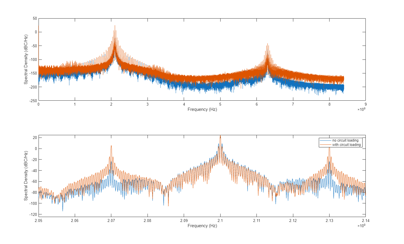
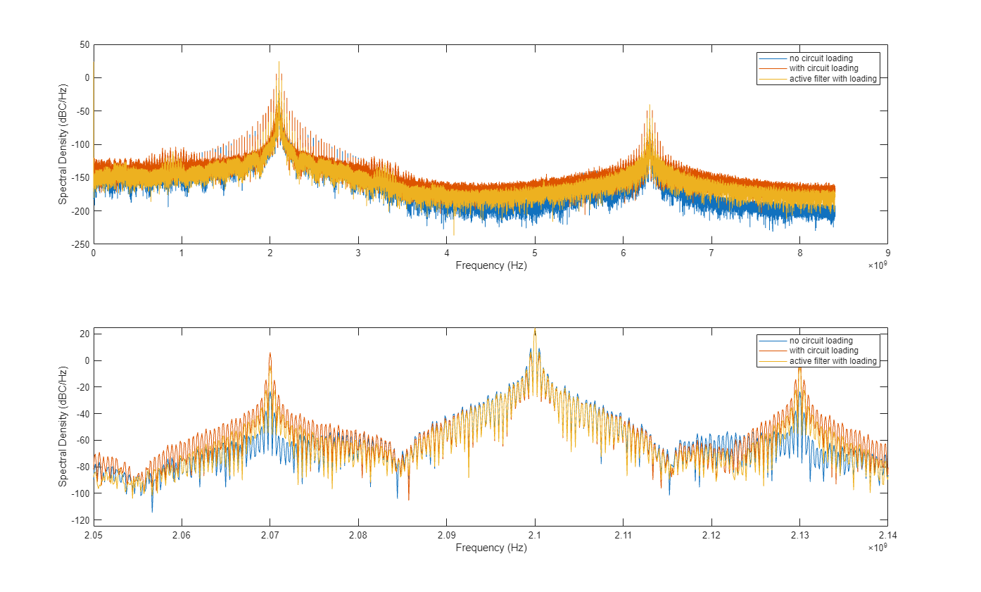
To plot the PLL output spectrum, you can use the plotPllOutputSpectrum helper script attached to this example. The resulting figures highlight the spurious responses at 30 MHz intervals due to the charge pump imbalance, and the output spectrum due to the reference phase modulation. You can create simulations that highlight other effects by modifying the level of these and other impairments.
plotPllOutputSpectrum(out,"no circuit loading");

Practical Circuit Design
Detailed circuit designs that include the effects of circuit element limitations and layout parasitics typically only become available late in the development of a product. At that time, you should incorporate the detailed circuit design of critical components into the system model to confirm that the as-designed system is ready for production.
As a simple example of the types of circuit effects that should be included in the detailed as-designed model, add a charge pump output impedance of 10 kΩ and a VCO control voltage input impedance of 100 kΩ to the third order passive filter model.

The associated circuit definition is provided in ThirdOrderCPLoading.slx.
schematic = "ThirdOrderCPLoading";
open_system(schematic);
cfg = cktconfig(schematic);

Plot the transfer functions of the new loop filter circuit.
figure(findobj(Type="figure",Tag="TF plot window"));
cktzpk(cfg,DisplayPlot=true);

To evaluate the effect of loop filter circuit loading, first delete the existing Loop Filter block, then create a new one based on the new schematic.
delete_block(model + "/" + block);
cktblock(cfg,model,CircuitDesignName=schematic,BlockName=block);
Connect the new Loop Filter block between the Charge Pump and VCO blocks.
set_param(model + "/" + block,Position=[730 226 900 284]);
Re-run the simulation to include the effect of circuit design details in the results.
The shape of the loop acquisition response has changed. There are more cycle slips during loop acquisition, but much less overshoot. The resulting lock time remains approximately the same as the lock time for the initial system design. Further, there is significantly more noise in the steady state loop filter output, and the additional noise appears to have a more or less constant amplitude.
out = sim(model);

Plot the PLL output spectrum using the plotPllOutputSpectrum helper script. The primary impact of the circuit loading is a substantial increase in the spurious responses.
plotPllOutputSpectrum(out,"with circuit loading");
Enhanced Circuit Design
In this loop filter design, the last RC section of the loop filter with loading is replaced by a Sallen and Keye active filter. This circuit design introduces a pair of resonant poles with a modest Q factor.

The associated circuit definition is supplied in FourthOrderActiveFilter.slx.
schematic = "FourthOrderActiveFilter";
open_system(schematic);
cfg = cktconfig(schematic);
Plot the transfer functions. Although the low frequency response closely resembles the response of the passive filter with loading, the high frequency response rolls off much more rapidly.
figure(findobj(Type="figure",Tag="TF plot window"));
cktzpk(cfg,DisplayPlot=true);
Click the Build/modify block button. The text on the block icon changes to match the revised circuit design name.
delete_block(model + "/" + block);
cktblock(cfg,model,CircuitDesignName=schematic,BlockName=block);
Connect the new Loop Filter block between the Charge Pump and VCO blocks.
set_param(model + "/" + block,Position=[730 226 900 284]);
Re-run the simulation to evaluate the effect of the active loop filter on the PLL system performance. The loop acquisition response is similar to those for the other cases studied but the loop filter output is much smoother.
out = sim(model);
Plot the PLL output spectrum using the plotPllOutputSpectrum helper script. The output spectrum reflects the improvements to the system performance. Specifically, the out-of-band spurious responses are dramatically reduced and the in-band response remains essentially unchanged.
plotPllOutputSpectrum(out,"active filter with loading");
References
1. Dean Banarjee. PLL Performance, Simulation, and Design, 4th edition.