Design Two-Stage Low Noise Amplifier Using Microstrip Transmission Line Matching Network
This example shows how to use the RF PCB Toolbox™ shapes and the pcbComponent object functionality to design a two-stage low noise amplifier (LNA) for a wireless local area network (WLAN) with an input and output matching network (MNW) to maximize the power delivered to the 50 ohm load.
Designing an input and output MNW is an important part of an amplifier design. The amplifier in this example has high gain and low noise. This example uses the traceTee RF PCB shape to create the input and output matching network.
The diagram shows the matching network topology used for both the input and output matching networks. The lengths and widths given in the paper[1] are for the lines TL2 and TL1 for Input MNW and TL3 and TL4 for the output MNW. Additional Port lines will be added as shown in the figure which will have same length as the series transmission lines(TL2 and TL3) so that we can connect the ports and analyze the structure. As the MNW forms the tee shape at both input and output, you can use the traceTee shape for creating the MNWs.

Define Microstrip Transmission Line Parameters
The microstrip transmission line parameters are chosen as follows.
Physical Height of conductor or dielectric thickness — 1.524 mm
Relative permittivity of dielectric — 3.48
Loss angle tangent of dielectric — 0.0037
Physical thickness of microstrip transmission line — 3.5 um
Create the Variables
The variables below are for creating the input and output MNWs. The Length_Line1 and Length_Line2 store the length of the series matching line and the length of the portline. The paper gives the TL2 as 14.7 mm and hence the portline at input also is taken as 14.7 mm. Hence the Length_Line1 becomes 29.4 mm. At the output MNW, the line TL3 is 22.5 mm and hence the portline at the output is also 22.5 mm. Hence Length_Line2 becomes 45 mm. The stub lengths Length_Stub1 and Length_Stub2 are also taken from the paper[1].
Length_Line1 = 29.4e-3; % Length of the Input Matching Network
Length_Stub1 = 8.9e-3;  % Length of the Stub

Length_Line2 = 45e-3;   % Length of the Output Matching Network
Length_Stub2 = 5.66e-3; % Length of the Stub
Width_Line   = 3.5e-3;  % Width of the line

EpsilonR     = 3.48;    % Dielectric EpsilonR
Height       = 1.524e-3;% Height of the Substrate
LossTangent  = 0.0037;  % Loss Tangent of the Substrate

fmin   = 2e9;
fmax   = 3e9;
points = 50;
freq   = linspace(fmin,fmax,points);
Use the nport function from RF Toolbox to read the sparameters of the amplifier from an s2p file for the amplifier and store it in the variables Amp1 and Amp2.
Amp1 = nport('f551432p.s2p');
Amp2 = nport('f551432p.s2p');
Design Input Matching Network Using tracetee shape
The input matching network consists of one shunt stub and one series microstrip transmission line. The dimensions of the series transmission line is Length_Line1 and the length of the stub is Length_Stub1. The width of the lines is Width_Line.
InputMatching = traceTee('Length',[Length_Line1 Length_Stub1],'Width',[Width_Line Width_Line]);
show(InputMatching);

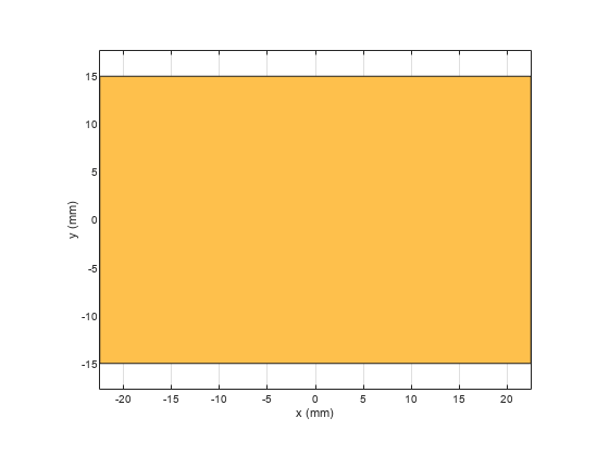
Gnd1 = antenna.Rectangle('Length',Length_Line1,'Width',30e-3);
show(Gnd1);

The output figures show the tee shaped matching network and the ground plane for creating the PCB stack.
Design Output Matching Network Using traceTee shape
The output matching network also consists of one shunt stub and one series microstrip transmission line. The dimensions of the series transmission line is Length_Line2 and the length of the stub is Length_Stub2. The width of the lines is Width_Line.
OutputMatching = traceTee('Length',[Length_Line2 Length_Stub2],'Width',[Width_Line Width_Line]);
figure;
show(OutputMatching);

Gnd2 = antenna.Rectangle('Length',Length_Line2,'Width',30e-3);
figure;
show(Gnd2);
The output figures show the tee shaped matching network and the ground plane for creating the PCB stack up.
Create pcbComponent for Input and Output Matching Networks
The pcbComponent method creates the PCB stack for any of the RF PCB shapes and it assigns the layers for dielectric, ground plane and feeds at the open ends of the shape.
Use the pcbComponent method to create the PCB stack of the InputMatching traceTee shape. Use the show method to visualize the PCB stack up of the traceTee. Notice that the pcbComponent method assigns the InputMatching shape, dielectric, ground plane to Layers property of pcbComponent and assigns FeedLocations at three open ends of the shape.
InputMatchingNw = pcbComponent(InputMatching);
figure;
show(InputMatchingNw);

The output shows the top and the bottom metal with the dielectric in the middle and ports at all the open ends of the shape. However the stub needs to be an open circuit. For this you can remove the feed at the third port, increase the ground plane width and change the dielectric values as per the paper[1] using the below code.
d=dielectric('Name',{'Teflon'},'EpsilonR',EpsilonR,'LossTangent',LossTangent,'Thickness',0.0016);
InputMatchingNw.Layers(2:3)          = {d,Gnd1};
InputMatchingNw.BoardShape           = Gnd1;
InputMatchingNw.FeedLocations(3,:)   = [];
InputMatchingNw.BoardThickness       = Height;
figure;
show(InputMatchingNw);
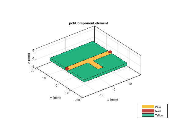
Observe the changes in the PCB stack up after removal of the feed and increasing the ground plane width.
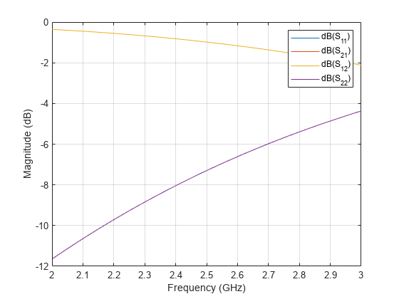
Use the sparameters function to calculate the s-parameters of the input matching network.
s_in=sparameters(InputMatchingNw,freq);
figure;
rfplot(s_in);
rfwrite(s_in,'s_in.s2p');Perform the same steps for the output matching network and build the required PCB stack.
OutputMatchingNw                      = pcbComponent(OutputMatching);
OutputMatchingNw.Layers(2:3)          = {d Gnd2};
OutputMatchingNw.BoardShape           = Gnd2;
OutputMatchingNw.FeedLocations(3,:)   = [];
OutputMatchingNw.BoardThickness       = Height;
figure;
show(OutputMatchingNw);
The output shows the top and the bottom metal with dielectric in the middle layer. Use the sparameters function to calculate the s-parameters of the output matching network.
s_out=sparameters(OutputMatchingNw,freq);
figure;
rfplot(s_out);

rfwrite(s_out,'s_out.s2p');Use nport function from RF Toolbox to import the s-parameter files for the input and output matching networks.
IMNW = nport('s_in.s2p');
OMNW = nport('s_out.s2p');
Cascaded Amplifier S-Parameters
Use the circuit function to cascade the two amplifiers and use the sparameters function to calculate the s-parameters and plot it using the rfplot method.
casamp = circuit([Amp2,clone(Amp2)],'amplifiers');
S2 = sparameters(casamp,freq);
figure;
rfplot(S2);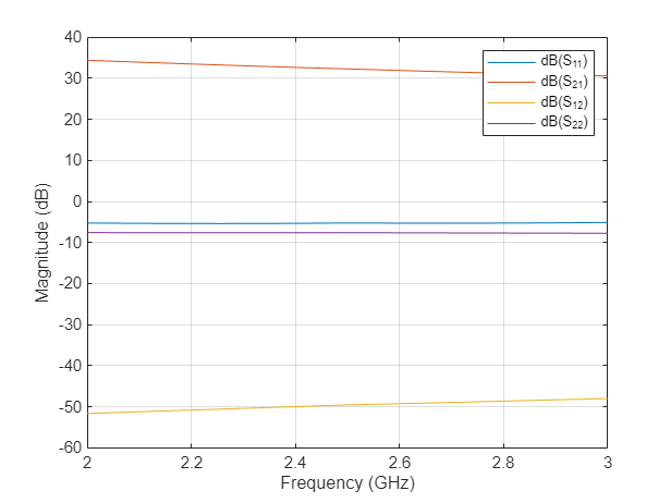
The plot shows that the S21 is around 35 dB but the S11 and S22 values are around -5 dB mark which is not sufficient as the expected values are -10 dB. So the MNWs that are designed will improve the S11 and S22 values.
Cascade Input and Output Matching Networks with Two Amplifiers
Use the circuit function to cascade the Input and output matching networks' s-parameters and the two amplifiers and plot the s-parameters. The S11 and S22 are below -10 dB indicating a proper matching at the input and output ports of the amplifier.
casamp1 = circuit([IMNW ,clone(Amp1),clone(Amp2), OMNW],'amplifiersWithMatching');
S3 = sparameters(casamp1,freq);
figure;
rfplot(S3);
The plot shows that the S11 and S22 are below -10 dB and hence the reflected power is reduced at Port1 and Port2.
Compare Input Reflection Coefficients of Two-Stage LNA
To verify the simultaneous conjugate match at the input of the amplifier, plot the input reflection coefficients in dB for the amplifier circuit with and without a matching network. Plot the s-parameters with and without the matching networks over the frequency range of 2 – 3 GHz.
figure;
rfplot(S2,1,1);
hold on;
rfplot(S3,1,1);
legend('|S11| of Two-Stage LNA Without MNW','|S11| of Two-Stage LNA with MNW');
title('Input Reflection Coefficients of Two-Stage LNA');
grid on;
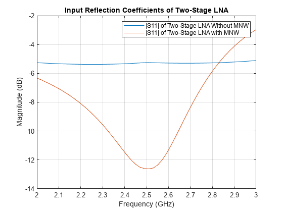
The input return loss for the two-stage LNA with the input MNW is around –12 dB.
Compare Output Reflection Coefficients of Two-Stage LNA
To verify the simultaneous conjugate match at the output of the amplifier, plot output reflection coefficients in dB for both the two-stage LNA with and without a MNW.
figure;
rfplot(S2,2,2);
hold on;
rfplot(S3,2,2);
legend('|S22| of Without MNW','|S22| of With MNW');
title('Output Reflection Coefficients of Two-Stage LNA');
grid on;

The calculated output return loss for the two-stage LNA with the output MNW is around -10 dB.
This matching network design can be used for matching any input impedance and convert that impedance to 50 ohm so that you get good matching at input and output.
Reference
[1] Maruddani, B, M Ma’sum, E Sandi, Y Taryana, T Daniati, and W Dara. “Design of Two Stage Low Noise Amplifier at 2.4 - 2.5 GHz Frequency Using Microstrip Line Matching Network Method.” Journal of Physics: Conference Series 1402 (December 2019): 044031.