Main Content

Register Channel

Timing model for transfer of register values

  • Register Channel block

Libraries:
SoC Blockset / Memory

Description

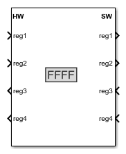
The Register Channel block provides a timing model for the transfer of register values between a processor and hardware logic. The register channel represents the datapath between a processor and a hardware IP via a common configuration bus. Configure the block to include one or more registers, and configure the direction for each register as write if the processor writes to it, or read if the processor reads from it.

Ports

Input

expand all

Each register is assigned a port pair: an input and an output. You can configure the processor to be a writer or a reader. If the register is a read register, then the input comes from the hardware (HW) side. If the register is a write register, the input comes from the software (SW) side. By default, the Nth register port is named regN. You can change a register name by clicking Edit in the Registers parameter dialog box.

Dependencies

The number of input ports depends on the number of registers in the register table.

Output

expand all

Each register is assigned a port pair: an input and an output. You can configure the processor to be a writer or a reader. If the register is configured as a read register, then the output goes to the software (SW) side. If the register is a write register, the output goes to the hardware (HW) side. By default, the Nth register port is named regN. You can change a register name by clicking Edit in the Registers parameter dialog box.

Dependencies

The number of output ports depends on the number of registers in the register table.

Parameters

expand all

This parameter includes a table, where each of its lines corresponds to a register in your IP. Edit the table to add or edit a register configuration, up to 32 registers.

For each register, you can edit these values:

  • Register Name – Specify the register name. This changes the input and output ports for this register.

  • Direction – Choose write if the processor writes the register. Choose read if the processor reads the register.

  • Data Type – Select the data type for the register. Supported data types are

    • single

    • int8

    • uint8

    • int16

    • uint16

    • int32

    • int64

    • uint32

    • uint64

    • boolean

    • fixdt(1,16,0)

    • fixdt(1,16,2^0,0)

    • fixed point

  • Dimension – Select the vector size of the register. The default value is 1.

This sample time represents the clock period on the hardware side. Specify an offset time by entering a two-element vector for discrete blocks or configurable subsystems. The first element is the sample time, and the second element is the offset time. For example, an entry of [1.0 0.1] specifies a 1.0-second sample time with a 0.1-second offset. If no offset is specified, the default offset is zero.

When the value is -1, the block inherits its sample time value from the model.

Note

When the Direction of a register is set to Write, it implies that software is the writer and hardware is the reader, but Register write sample time determines the sample time of the signal on the hardware side.

Extended Capabilities

Fixed-Point Conversion
Design and simulate fixed-point systems using Fixed-Point Designer™.

Version History

Introduced in R2019a