Get Started with RFSoC Devices
This example shows how to get started with modeling wireless applications and implementing them on AMD® Zynq® UltraScale+™ RFSoC devices.
Introduction
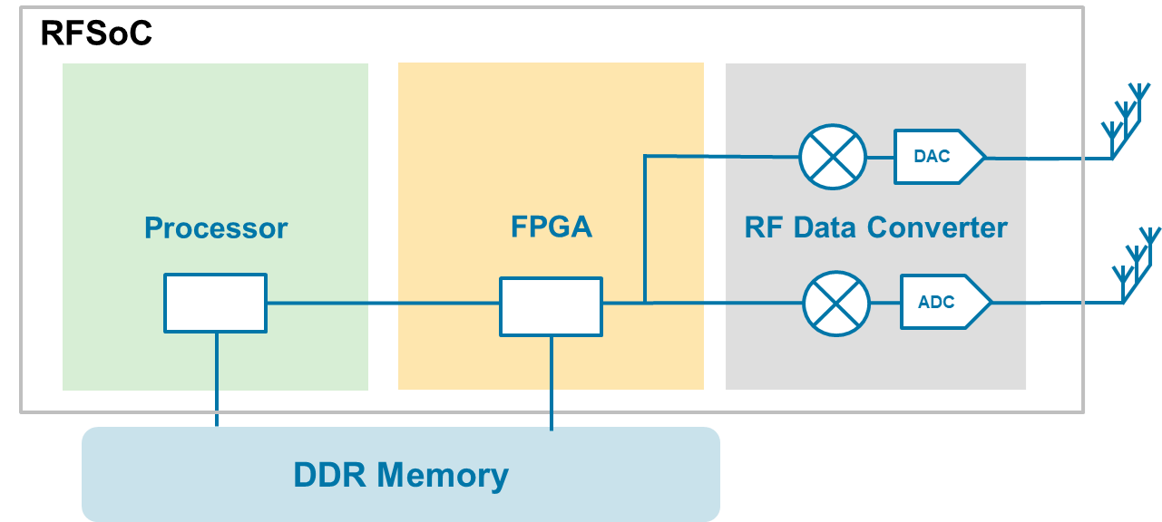
RFSoC integrates an RF data converter, an ARM® processor, and an FPGA fabric to optimize performance and power consumption for wireless applications. RFSoC applications often use external memory for high data rate processing. SoC Blockset™ provides a Model-Based Design workflow to accelerate RFSoC application development.
Create RFSoC Project
To open the SoC Blockset template page, open Simulink and scroll down to the SoC Template area.
To create a new RFSoC project in your selected folder, locate the RFSoC template and click Create Project.
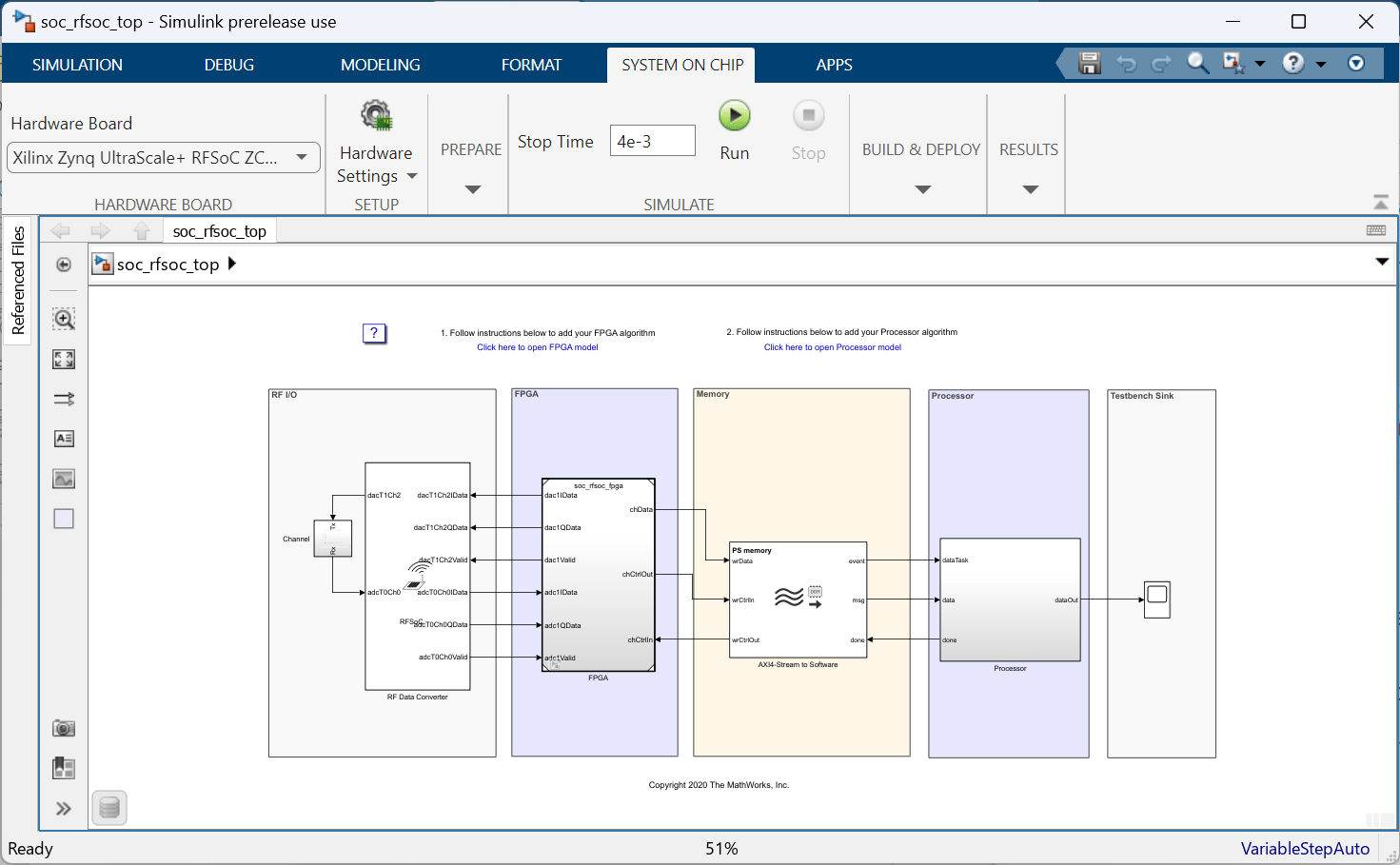
To open the model, double-click
soc_rfsoc_top.slxin your project folder.
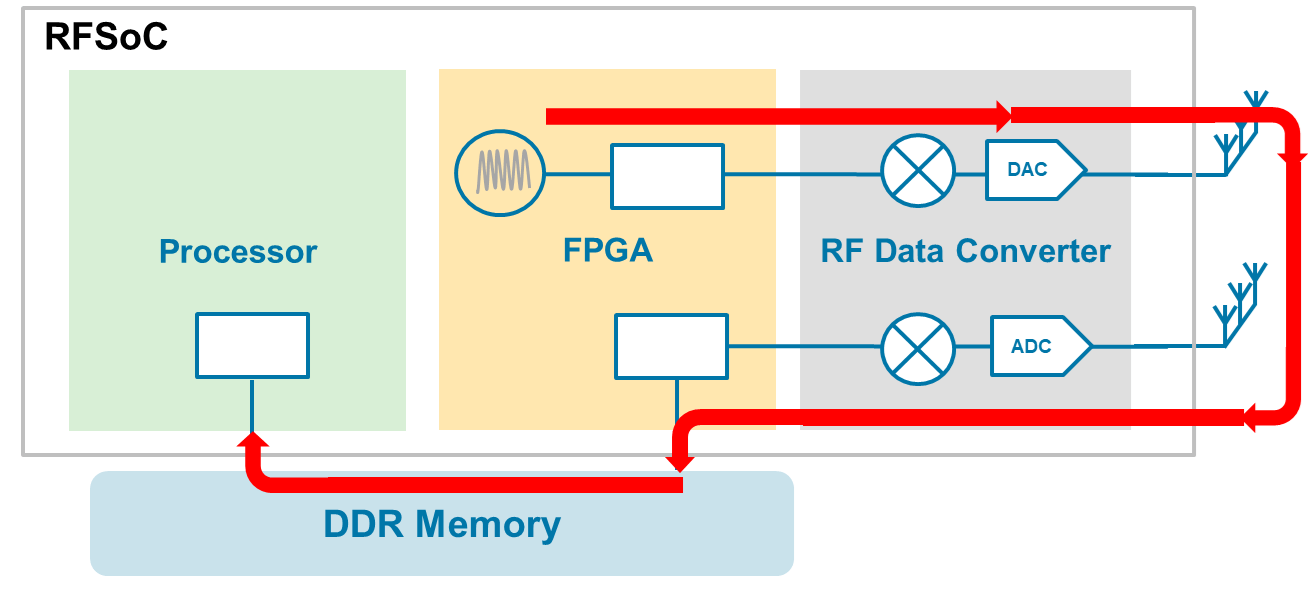
The RFSoC project template implements a loopback from the FPGA to the processor through the RF Data Converter block.
The template includes three Simulink models:
SoC top model (
soc_rfsoc_top.slx) — Defines the architecture of the RFSoC application. It includes hardware component models for the FPGA and the processor connected with interface, I/O, or testbench blocks. The RF Data Converter block models the RF Data Converter IP component. The AXI4-Stream to Software block models the memory interface between the FPGA and the processor.FPGA model (
soc_rfsoc_fpga.slx) — Implements the FPGA HDL algorithm.Processor model (
soc_rfsoc_processor.slx) — Implements the software algorithm.
Select Hardware Board
By default, the template for this RFSoC project specifies Xilinx Zynq UltraScale+ RFSoC ZCU111 as the hardware board to use. You can specify a different hardware board, however, you must reconnect the ports on the RF Data Converter block to accommodate differing ADC and DAC tiles. To change the selection, follow these steps:
From the SoC top model (
soc_rfsoc_top.slx), navigate to the System on Chip tab and set Hardware Board to a supported board. For a list of supported boards, see Supported Xilinx Devices. Note: Changing the hardware board requires reconnection of the RF Data Converter block ports due to ADC/DAC tile difference.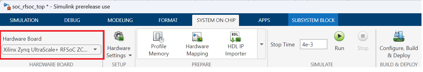
Open the FPGA model (
soc_rfsoc_fpga.slx) by clicking the icon in the bottom-left corner of the FPGA model block. Specify the same hardware board as in SoC top model and save your selection. Open the configuration parameters panel by clicking the Hardware Settings button and set the Processing Unit parameter toFPGA.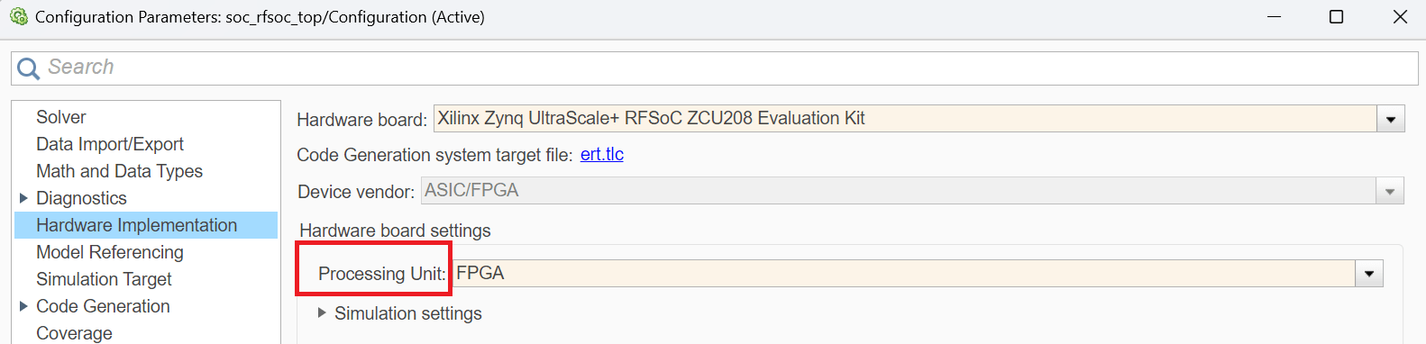
Open the processor model (
soc_rfsoc_processor.slx) by clicking the icon in the bottom-left corner of Processor - Frame based processing model block. Specify the same hardware board as in the SoC top model and save your selection. Open the configuration parameters panel by clicking the Hardware Settings button and set the Processing Unit parameter toAPU.
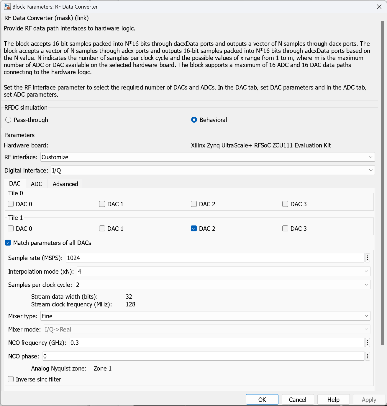
Configure RF Data Converter
Plan the frequency spectrum according to your RF requirements. The default settings in the RFSoC project template are:
DAC — 1024 MSPS, 2 samples per clock, NCO frequency 0.3 GHz
ADC — 1024 MSPS, 2 samples per clock, NCO frequency –0.3 GHz
Configure these parameters in the RF Data Converter block mask.
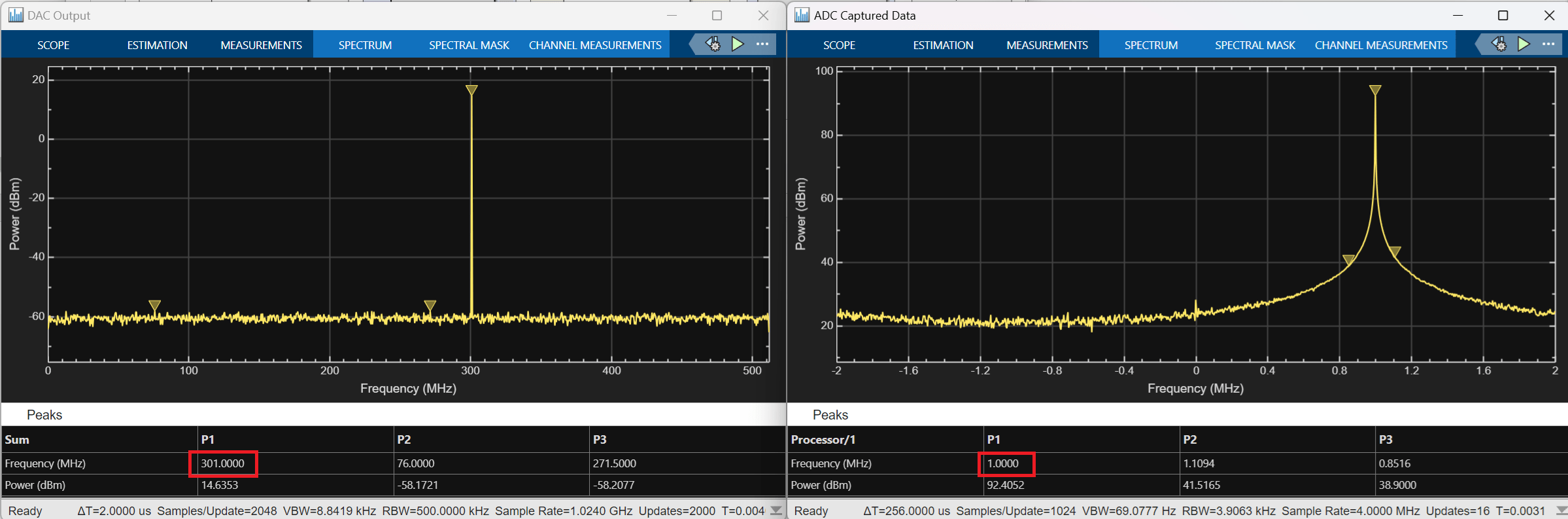
Run Simulation
Open the SoC top model and, on the System on Chip tab, click Run.
Verify that the RF data converter behavior matches your frequency plan. For example, check that the frequency shifted 300 MHz in the DAC output spectrum because of the mixer.
Set Up Hardware Board
Make sure the required daughtercards or loopback cards are assembled on the evaluation boards.
Loop back the configured DAC and ADC channels on the RF loopback card for the board you selected.
Open the Hardware Setup app to create the SD card and boot your evaluation board. For more information, see Set Up AMD FPGA and SoC Devices.
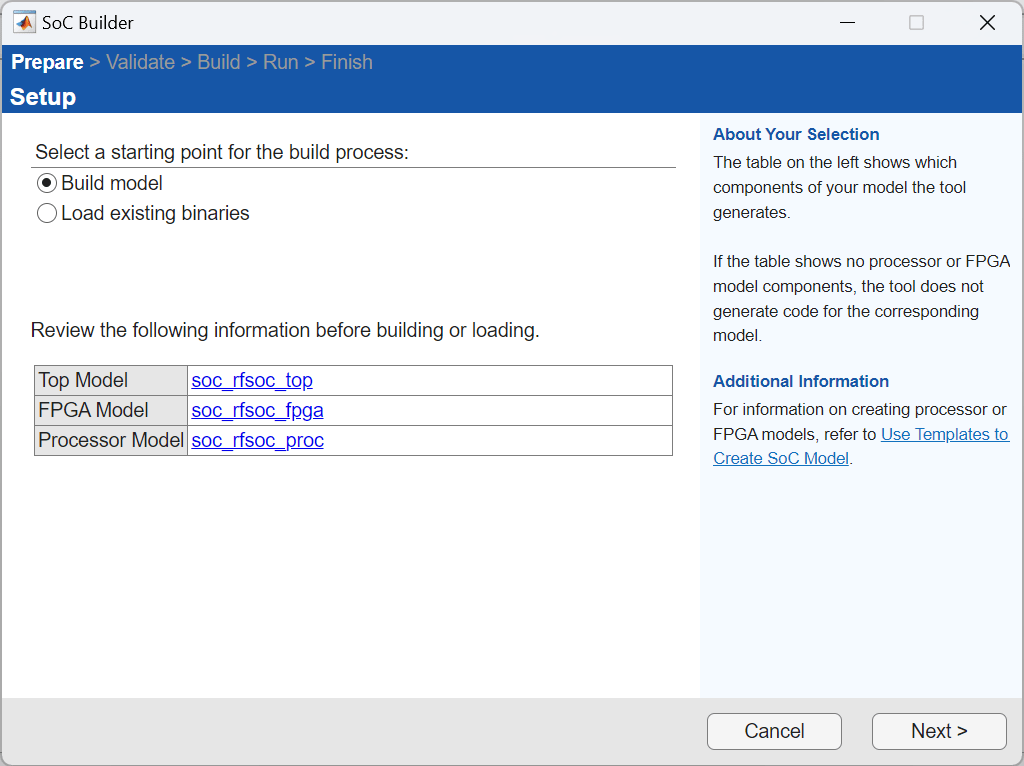
Deploy to Hardware Board
To start SoC Builder, open SoC top model (
soc_rfsoc_top.slx), and click the Configure, Build and Deploy button on the System on Chip tab.Follow the steps in SoC Builder to build and run the application on the RFSoC hardware board.
Optional: if you choose Build and load for external mode in the Select Build Action step, click Monitor & Tune on the generated software model (
soc_rfsoc_top_sw.slx) to run the software application in external mode.
Conclusion
This example shows how to get started with RFSoC application design and implementation. Modify the implementation for your use cases and explore other application examples for 5G and Radar as references.