Model DAC and ADC for Signal Conversion on STM32 Processor
This example shows how to use the Digital to Analog Converter (DAC) and Analog to Digital Converter (ADC) blocks to model DAC and ADC peripherals in Simulink® models targeting STM32 processor-based boards. The DAC block converts digital values into analog voltages, and the ADC block converts analog voltages into digital values.
Model Design and Configuration
Consider example model gettingStartedDAC.slx.
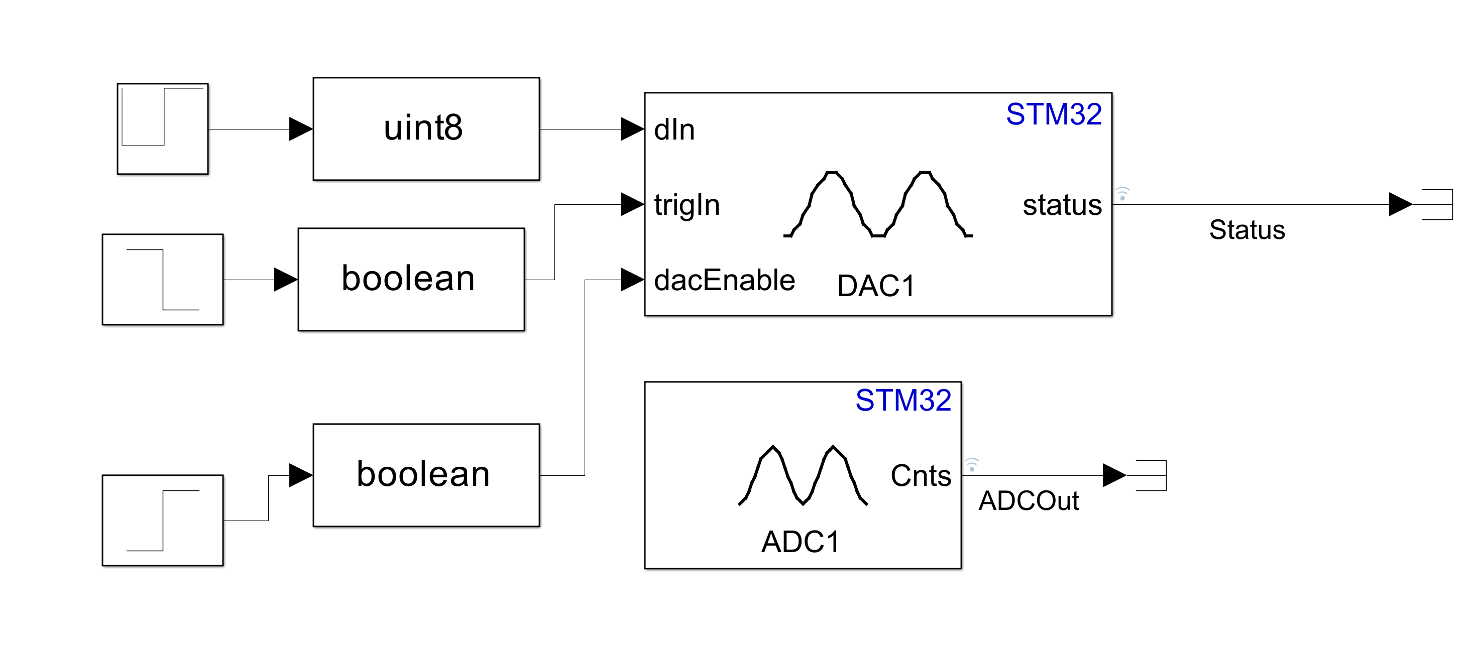
A Repeating Sequence block and two Step blocks pass data (
dIn), trigger (trigIn), and DAC enable (dacEnable) values as input to the Digital to Analog Converter block.
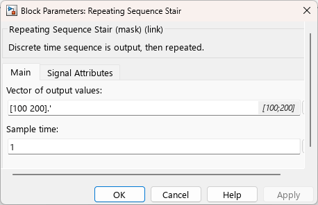
The Repeating Sequence block is configured to source vector output values of 100 and 200 at a sample rate of one second.
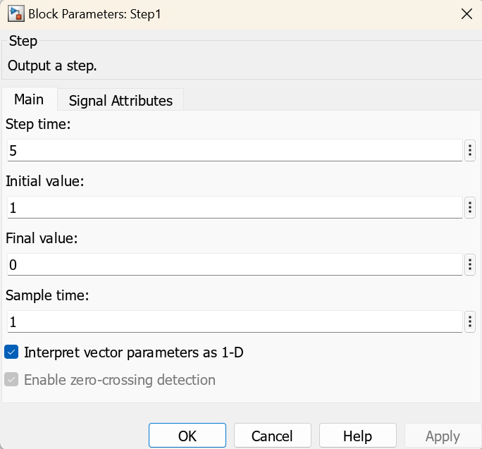
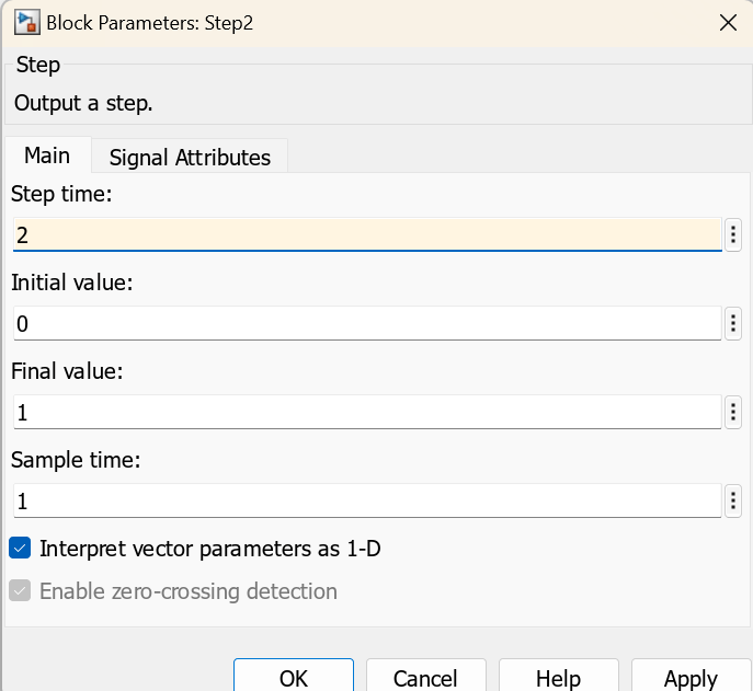
The Step block that provides the trigger input is configured to initiate a trigger signal after five seconds..
The Step block that provides the DAC enable input is configured to enable conversions every two seconds.
Set Up Hardware Connections
To use this example, connect the DAC output to the ADC input externally on the hardware.
Configure Peripherals
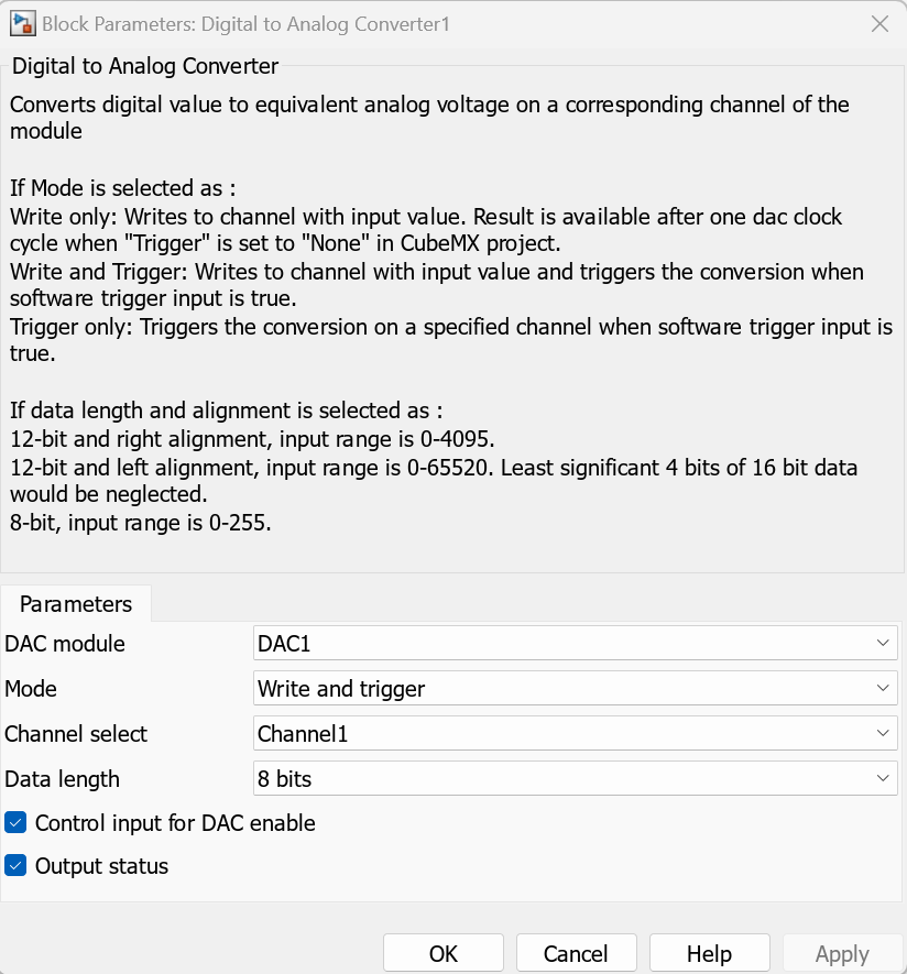
The Digital to Analog Converter block (DAC1) is configured to operate in Write and trigger mode, using channel 1 and a data length of 8 bits. The block writes a digital input value to channel 1 and triggers a conversion to an analog voltage when the value of the trigger input (trigIn) is true.
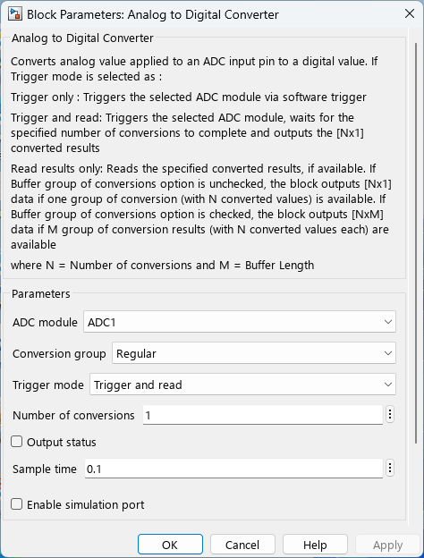
The Analog to Digital Converter block (ADC1) is configured to operate in Trigger and read mode, using the regular conversion group and a conversion count of 1.
The Digital to Analog Converter and Analog to Digital Converter blocks are short circuited with Terminator blocks.
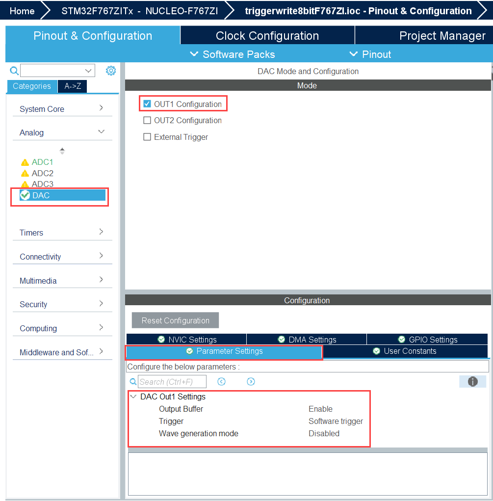
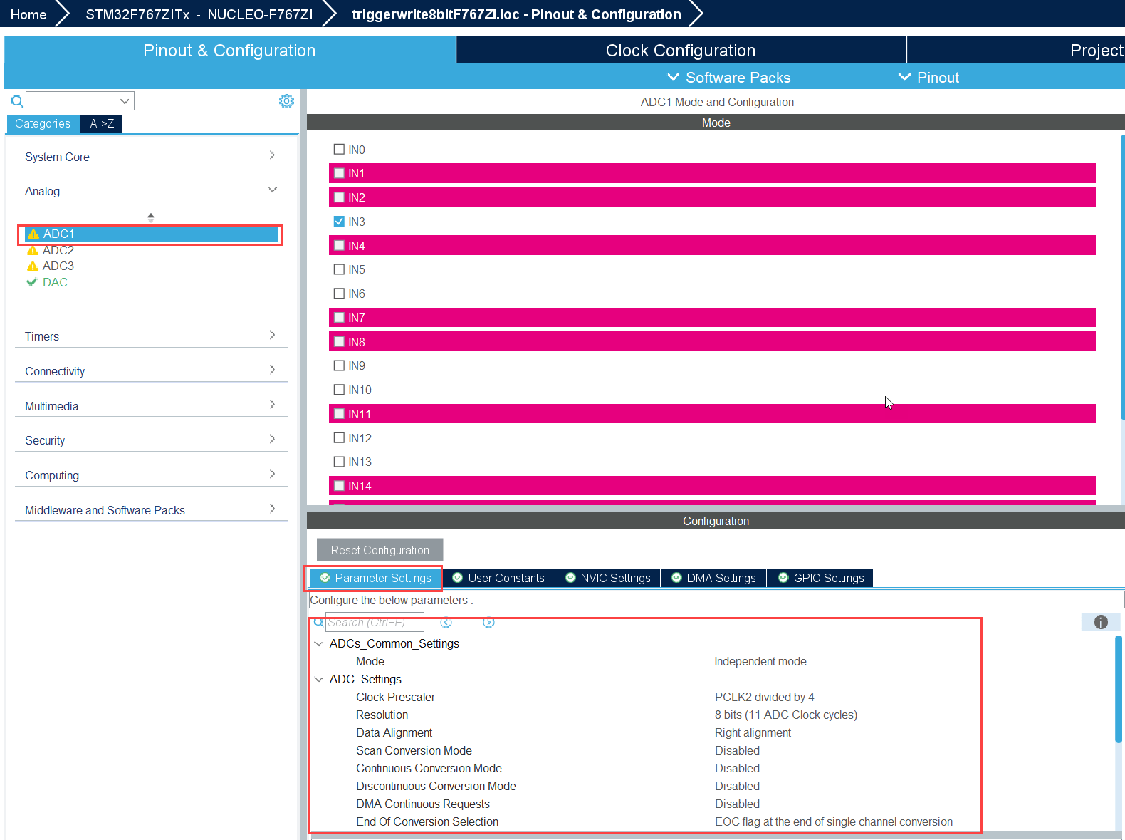
Configure STM32CubeMX IOC
Open the triggerwrite8bitF767ZI.ioc file and configure the ADC and DAC peripherals as shown.
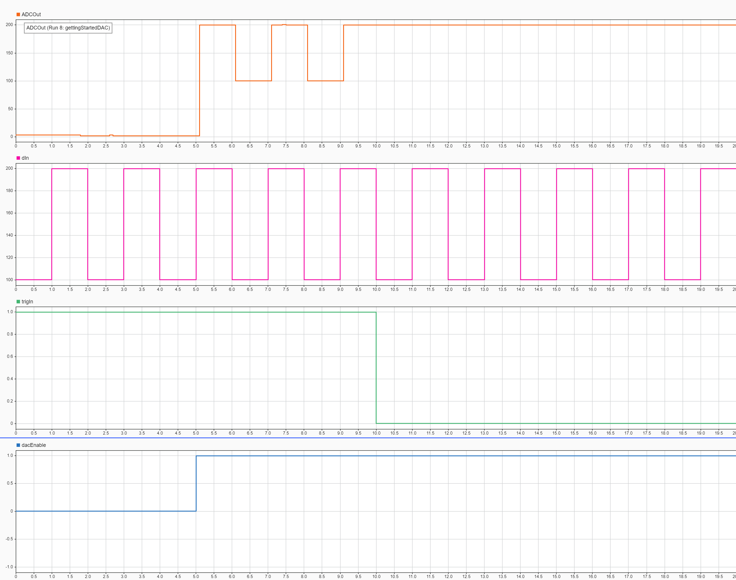
Simulation Results
This Simulation Data Inspector view shows the simulation results for model gettingStartedDAC.slx.
From zero to five seconds, the value of
dacEnableis0. This causesADCOutto remain0during that time period regardless of the data provided bydIn.From five to ten seconds,
dacEnableis1and the value oftrigInis1, indicating that the DAC is active and updating. During that time period,ADCOutfollows the pattern ofdIn, which is to rise from100to200, after one second, fall from200to100, and repeat.After ten seconds,
trigInfalls to0, causing the DAC to stop updating and hold the last value of200, even thoughdIncontinues to fall and rise.