TLM Component Architecture
Overview of Component Features
The TLM generator exports a target TLM component from a Simulink® model subsystem. The target TLM component has a single TLM socket that supports read and write transactions using the TLM generic protocol and generic payload.
Note
This feature requires the ASIC Testbench for HDL Verifier add-on.
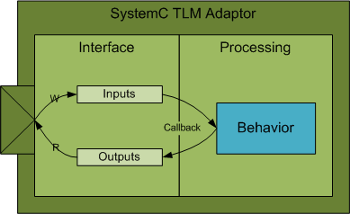
The following diagram illustrates the simplest behavior you can specify for the generated TLM component. It contains no memory map or command and status register, and executes transactions immediately.

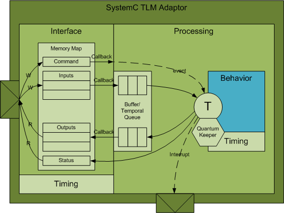
To control the architecture of the generated TLM component, you can choose among several options. Incorporating a memory map is one of the most effective options. The following figure demonstrates the behavior of a generated TLM component with a full complement of features enabled.

You can set options for the following TLM component features:
Interface Timing — Model time used by transactions in a real system.
Algorithm Execution — Implement the component as a SystemC™ thread or a callback function.
Memory Mapping
No Memory Map
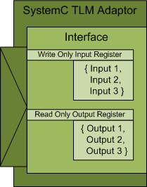
The no memory map option generates a TLM component with only one read and one write register without any address. The Simulink model inputs are represented by the write register and the outputs are represented by the read register.


Without a memory map, the generated TLM component has the following characteristics:
Has a single input register and a single output register.
Does not need—and ignores—an address in the read and write requests during SystemC simulation to select specific registers on the device.
Receives all input data in a single write request, and a read request receives all output data in the return value
Has input and output registers either sized to hold an entire data set required or created by the TLM component when it executes the behavior (algorithm step function) in your virtual platform environment
When input registers are full, this condition triggers (schedules) execution of the behavior in the SystemC simulator. Output registers are handled the same way.
All defaults for commands and status are applied.
When you generate the TLM component with this option, you can use it in a virtual platform (VP) as:
A standalone component in a verification testbench
A direct bound co-processing unit
A device attached to a communication channel using a protocol adapter
Automatically Generated Memory Map with Single Address
The automatically generated memory map with single address option generates a TLM component with only one read data register and one write data register with one address each.


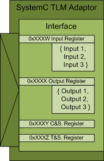
The Simulink model inputs are represented by the write register, and the outputs are represented by the read register. HDL Verifier™ software automatically assigns the addresses required to access those specific registers during code generation. Those addresses give the specific offsets required to address each individual register via read and write operations. Definition of the base address for the entire generated TLM component should be defined by the virtual platform that the TLM component resides in. The offset address definitions appear in a definition file that is generated along with the TLM component.
With a single address memory map, the generated TLM component has the following characteristics:
Has a single input register and a single output register, and optional command and status register and test and set register.
Must have an address in the read and write requests during SystemC simulation to select specific registers on the device.
Receives all input data in a single write request, and a read request receives all output data in the return value
Has input and output registers either sized to hold an entire data set required or created by the TLM component when it executes the behavior (algorithm step function) in your virtual platform environment
If a command and status register is not used or if the command and status register is used and the default values apply, when input register is full, content is pushed into buffer, which then triggers (schedules) execution of the behavior in the SystemC simulator. If the command and status register is used and the Push Input Command is set to 1, the initiator module moves the input data set from the input register to the input buffer. Output registers are handled the same way.
If a command and status register is not used, all defaults for commands and status are applied.
When you generate the TLM component with this option, you can use it in a virtual platform (VP) as a standalone component in a testbench, or you can attach it to a communication channel.
Automatically Generated Memory Map with Individual Addresses
The automatically generated memory map with individual address option generates a TLM component with one read data register per model output and write data register per model input with individual addresses.


Each Simulink model input is represented by its corresponding write register, and each output is represented by its corresponding read register. HDL Verifier software automatically assigns the addresses required to access those specific registers during code generation. Those addresses give the specific offsets required to address each individual register via read and write operations. Definition of the base address for the entire generated TLM component should be defined by the virtual platform that the TLM component resides in. The offset address definitions appear in a definition file that is generated along with the TLM component.
With an individual address memory map, the generated TLM component has the following characteristics:
Each input register and each output register has its own address as well as an optional command and status register and test and set register.
Must have an address in the read and write requests during SystemC simulation to select specific registers on the device.
Each input and output register must be accessed individually.
Initiator module can write or read each input and output register in multiple and/or partial transactions.
The size of each input and output register is the size of the data.
Execution is triggered when all input has been written or when command and set register bits are set to Automatic. If set to manual, the initiator module moves the input data set from the input register to the input buffer.
Output registers are refreshed when all output registers have been read or when command and set registers bits are set to Automatic. If set to manual, the initiator module moves the output data set from the output buffer to the output register.
When you generate the TLM component with this option, you can use it in a virtual platform (VP) as a standalone component in a testbench, or you can attach it to a communication channel.
Command and Status Register
You can choose to generate a TLM component with an automatically generated memory map with addresses. When you do so, the TLM generator offers you the option to incorporate a Command and Status register (CSR) in the generated TLM component. The definition for this register appears in the table.
Write-Only Bits
Write-only (WO) bits assert mutually exclusive commands. You can assert only one command bit in any single write operation to the CSR. If more than one command bit is set in the write to the CSR, the command is undefined. You activate each command by writing a 1 to a command bit in the register. Then, each command bit is automatically cleared after the command has been executed. You do not have to write a 0 to the register to clear a command bit. Write-Only bits are always returned as 0 in any read of the CSR. Writing a command does not overwrite the Read/Write or Write-Only bits.
Read-and-Write Bits
Use Read and Write (R/W) bits to obtain the current status and setting. R/W bit are sticky, meaning that after you set them by writing a 1 to the bit in the register, an R/W bit remains set until a 0 is written to the same bit or the Reset command is invoked. Read-and-Write bits return their actual values to any read of the CSR.
A single write operation to the CSR sets all Read-and-Write bits in the register. You can choose to set only some of the bits and maintain the previous values of others. Before you do so, you must first read the CSR and then modify the values according to your requirements. After you complete modifications, you can write the entire 32 bits back to the CSR.
Read-Only Bits
Read-Only (RO) bits provide status information. The generated TLM component automatically sets and clears their values, and an initiator module can read them to learn status. Read-Only bits do not change their actual values during any read or write of the CSR.
Register Definition
The following table contains the entire register definition.

The following table explains how the bits are defined.
| Bit | Name | Read/Write Status | Description |
|---|---|---|---|
| CSR<0> | Reset Command | Write-only | When set to 1, the following are true:
Automatically returns to 0 after command execution. |
| CSR<1> | Start Command | Write-only | Manually triggers execution of the TLM component behavior using the input data set that is currently in the input register when there is no input buffering. When input buffering is used, this command is undefined. |
| CSR<2> | Interrupt Status | Read-only | Reflects the current state of the Interrupt signal. Provides status only. Sets and clears itself automatically. |
| CSR<3> | Interrupt Disable | Read-and-write | When set to 0, allows interrupts to be generated on the Interrupt signal and reflected in the Interrupt Status bit of the CSR. When set to 1, disables generation of interrupts. |
| CSR<8> | Push Input Command | Write-only | When buffering is used and the Input Mode is equal to 0 (manual mode), this command allows an initiator module to move the input data set from the input register to the input buffer. It then triggers execution of the TLM component behavior. When buffering is not used, this command is undefined. When Input Mode is 1 (automatic), this command is undefined. |
| CSR<9> | Input Mode | Read-and-write | When set to 1 (automatic), movement of the input data set from the input register to the input buffer and execution of the TLM component behavior is triggered automatically, if a complete data set has been written to the input register. When set to 0 (manual), movement of the input data set from the input register to the input buffer and execution of the behavior must be manually initiated. Do so by writing the Start Command bit to 1, if no buffering is used, or writing the Push Input Command to 1, if buffering is present. By default the Input Mode is set to 1 (automatic). To change it to 0 (manual), specify it in the TLM component constructor parameters. |
| CSR<12> | Pull Output Command | Write-only | When buffering is used and the Output Mode is set to 0 (manual mode), this command allows an initiator module to move the output data set from the head of the output buffer to the output register. When buffering is not used, this command has no effect. When Output Mode is 1 (automatic), this command is undefined. |
| CSR<13> | Output Mode | Read-and-write | When set to 1 (automatic), movement of data from the head of the output buffer to the output register is triggered automatically by the execution of the TLM component behavior. When set to 0 (manual), movement of data from the head of the output buffer to the output register must be manually initiated. Do so by writing the Pull Output Command to 1, if buffering is present. By default the Output Mode is set to 1 (automatic). To change it to 0 (manual), specify it in the TLM component constructor parameters. |
Interrupt
You can add an interrupt signal added to the generated TLM component. The TLM component asserts this signal whenever new outputs are available in any output register. The signal is automatically cleared whenever a value is read from any output register.
The Interrupt signal is a SystemC Boolean signal active high. The Interrupt Active bit in the Status Register reflects the state of the interrupt signal.
Test and Set Register
You can use the optional test and set register to control access to a shared TLM component in your SystemC environment. Any read of this register returns the current value and sets the register to a new, asserted value in an atomic operation. In systems with multiple initiator modules, executing this task usually requires access to the same target. If so, then an initiator module has exclusive access to the generated TLM component, as long as all other initiator modules follow. The initiator modules must read the test and set register and use the target device only when that read operation returns a value of 0. An initiator module can verify that any subsequent read of the test and set register returns a value of 1, which indicates to other initiator modules that the device is busy. After gaining exclusive access to the TLM component, an initiator module releases the component when the target operations complete by writing a 0 to the test and set register.
Registers and Signal Ports
Registers
The TLM component reads and writes inputs and outputs directly from the interface register during algorithm processing. After the initiator writes all input registers (if in AUTO mode) or when the initiator writes the START command in the CSR, the algorithm begins processing. A SystemC wait function generates all timings.
Caution
To prevent corruption of the algorithm processing results, do not allow an initiator to perform a read or write of the registers during processing.
This diagram shows a TLM Adaptor with registered interfaces.

Signal Port
The TLM Component reads and writes inputs and outputs through a
sc_signal port (sc_in or sc_out).
These inputs/outputs are not registered. When the step function is executed, it reads the
current value of the sc_in ports, executes and writes the result in the
sc_out ports.
This diagram shows a TLM Adaptor with register interfaces, and an sc_in
port (in red).
