Bandstop and Bandpass Filters with Open Microstrip Line Stubs Using Behavioral and EM Simulation
This example shows different ways to create microstrip Line bandpass and bandstop filters using open circuit stub.
Convert the RF PCB catalog into a circuit element using a pcbElement object and build a Tee shaped circuit. Analyze the circuit using the behavioral model and EM simulation. Use the traceTee shape object in RF PCB Toolbox to create a tee shaped trace. Convert the shape into a PCB component and analyze it. Analyze the PCB using EM Simulation and compare the results with the circuit counterpart.
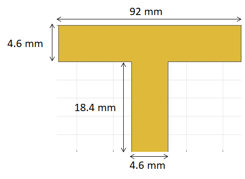
The dimensions of the microstrip line and the stub in the figure are taken from the reference. The left image shows the circuit representation with the port numbers and the right side image shows the traceTee structure with same dimensions.

Circuit Element with Behavioral Model for Microstrip Line
Create a circuit object and three microstripLine objects to build the circuit as shown in the figure. Update the value of EpsilonR and Height to 2.33 and 1.57 mm respectively.
ckt = circuit;
c1 = microstripLine('Length',46e-3,'Width',4.6e-3,'Height',1.57e-3);
c1.Substrate.EpsilonR = 2.33;

c2 = microstripLine('Length',46e-3,'Width',4.6e-3,'Height',1.57e-3);
c2.Substrate.EpsilonR = 2.33;

c3 = microstripLine('Length',18.4e-3,'Width',4.6e-3,'Height',1.57e-3);
c3.Substrate.EpsilonR = 2.33;
Use the pcbElement object to convert the microstrip lines to circuit objects and set the Behavioral flag to true so that the computation is done using the analytical equations. In the circuit model, the microstrip discontinuities are not modelled, hence the results might be slightly different from EM analysis.
p1  = pcbElement(c1,'Behavioral',true);
p2 = pcbElement(c2,'Behavioral',true);
p3 = pcbElement(c3,'Behavioral',true);
Use the add function to form the circuit and use the ports numbers as shown in the circuit above. Use port numbers 1 and 2 for the first microstrip line and connect another microstrip line from ports 2 to 3 which forms a series connection. Connect the third microstrip line from the port 2 to 4 which forms a tee network.
add(ckt,[1 2 0 0],p1);
add(ckt,[2 3 0 0],p2);
add(ckt,[2 4 0 0],p3);
setports(ckt,[1 0],[3 0]);
Use the sparameters function to calculate the s-parameters for the circuit and plot it using the rfplot function.
S = sparameters(ckt,linspace(1e9,10e9,21));
figure,rfplot(S);
Circuit Element with EM simulation for Microstrip Line
Use the pcbElement object to convert the microstrip lines to circuit objects and set the Behavioral flag to false so that the computation is done using EM Simulation.
ckt1 = circuit;
p1   = pcbElement(c1,'Behavioral',false);
p2   = pcbElement(c2,'Behavioral',false);
p3   = pcbElement(c3,'Behavioral',false);
Use the add function to form the circuit and use the port numbers as shown in the circuit above. Use port numbers 1 and 2 for the first microstrip line and connect another microstrip line from ports 2 to 3 which forms a series connection. Connect the third microstrip line from the port 2 to 4 which forms a tee network.
add(ckt1,[1 2 0 0],p1);
add(ckt1,[2 3 0 0],p2);
add(ckt1,[2 4 0 0],p3);
setports(ckt1,[1 0],[3 0]);
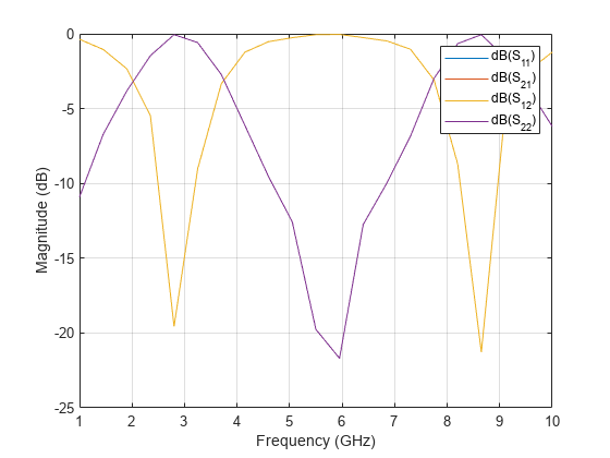
Use the sparameters function to calculate the s-parameters for the circuit and plot it using the rfplot function. Each microstripLine section is solved using the EM solver and the s-parameters calculated are combined to give the combined response of the circuit.
S = sparameters(ckt1,linspace(1e9,10e9,21));
figure;
rfplot(S);

Creating PCB Stack of traceTee Shape with EM Simulation
Use the traceTee shape to create the open circuit stub and use the dimensions as shown in the figure above and visualize it.
obj = traceTee;
obj.Length = [92e-3 18.4e-3];
obj.Width  = [4.6e-3 4.6e-3];
figure;
show(obj);

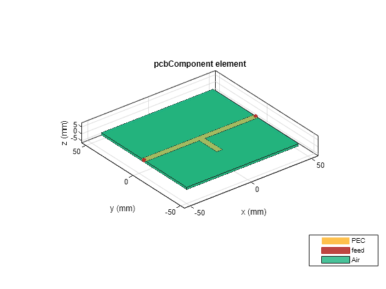
Use the pcbComponent to convert the shape into a PCB stack. The pcbComponent creates the PCB stack up for traceTee shape and assigns the FeedLocations at the three open ends of the shape. Assign the dielectric and groundplane to the Layers property of the pcbComponent. Also assign the BoardShape to the grounplane. In the current design, the stub is required as open circuit, hence delete the feed at the third location.
pcb = pcbComponent(obj);
gnd = traceRectangular('Length',obj.Length(1),'Width',90e-3);
d   = dielectric('EpsilonR',2.33);
d.Thickness = 1.57e-3;
pcb.BoardThickness = 1.57e-3;
pcb.Layers{2}      = d;
pcb.Layers{3}      = gnd;
pcb.BoardShape     = gnd;
pcb.FeedLocations(3,:)=[];
figure;
show(pcb);
Use the mesh function to manually mesh the structure and set the MaxEdgeLength to 10 mm.
figure,mesh(pcb,'MaxEdgeLength',10e-3);
Use the sparameters function to calculate the s-parameters of the structure and plot it using rfplot function.
S1 = sparameters(pcb,linspace(1e9,8e9,35));
figure;
rfplot(S1);

Design at Specific Frequency
The resonance of the bandstop filter depends on the stub length which needs to be quarter wavelength at the resonant frequency. In the above example the stub is quarter wavelength at 2.9 GHz and hence is resonance is observed at that frequency. If the resonance is expected at any other frequency then the stub length needs to be quarter wavelength at that frequency.
References
Alexander B. Yakovlev, Ahmed I. Khalil , Efficient MOM-based generalized scattering matrix method for the integrated circuit and multilayered structures in waveguide