Timing Analysis
The Parallel Link Designer app has an integrated static timing analysis engine capable of computing setup and hold timing margins on synchronous (common-clock) and source-synchronous transfers. It can support both single data rate (SDR) and double data rate (DDR) signaling.
You can define the timing relationships and constraints in the component timing models. The app uses the timing models to determine what type of timing analysis to perform. Timing analysis also depends on etch delays, clock skew, UI, jitter, and transfers.
Timing Model
A timing model template is a file that has the correct model structure and syntax, and
has all of the pin information. The timing model template generator parses an existing IBIS
model and creates a timing model that contains entries for each pin, in vector notation,
already sorted by pin type (input, output, or bidirectional.) You may add existing timing
models by copying the files to the <project path>/si_lib/timing
directory.
You can create a new timing model from scratch, but it is recommended that you start from an automatically generated timing model template.
Generate Timing Model Template
To generate a timing file template, open the Edit Part Properties dialog box by clicking Libraries > Edit Part Properties from the app toolstrip and selecting a part properties file. Timing model template generation uses the IBIS component, so you must specify the IBIS file. Click the Generate button below the Timing File parameter. You can also rename the base name of the timing model file.
Timing Model Syntax
The format of a timing model is:
MODEL: <name>
DESCRIPTION: <description>
SOURCE: <source>

PARAMS:
<parameter definitions>
END_PARAMS

PINDEF: 9 PINS
INPUTS
<pin groups>
OUTPUTS
<pin groups>
BIDIR
<pin groups>
UNINTERESTING
<pin groups>
END_PINDEF

<timing statements>

END_MODEL
Timing Model Keywords
| Field | Keyword | Required | Description | Syntax Rule |
|---|---|---|---|---|
| General | MODEL | Yes | The start of the model specified by the file name. The model name is used in part properties and transfer net files. | |
DESCRIPTION | No | The description of the model. | ||
SOURCE | No | The source of the model, for example, creator. | ||
| Parameters | PARAMS | No | The start of the list of parameter assignment statements. | |
END_PARAMS | No | The end of the list of parameter assignment statements. | ||
| Pin definition | PINDEF | Yes | The start of the pin definition section. | You can add arbitrary strings at the end. For example: PINDEF <package_name> <number_of_pins> |
INPUTS | No | The list of the PIN_NAME inputs. | ||
OUTPUTS | No | The list of the PIN_NAME outputs. | ||
BIDIR | No | The list of the PIN_NAME bidirectional. | ||
UNINTERESTING | No | The list of the PIN_NAME that are not involved in the
timing for this part. | ||
END_PINDEF | Yes | The end of the pin definition section. | ||
| Timing statements | DELAY | One of these is required | The delay from the clock input pin to data output pin. It uses both min and max delay values for each process corner (FF, TT, SS). | Define the reference clock edge, clop and data pin names, and delays. DELAY<*> <clk_edge> <clk_pin> *TO <data_pin> <delays> |
DELAY_CORRELATED or DELAY_C | The delay from the clock input pin to data output pin.
| |||
DELAY_ANTI_CORRELATED or
DELAY_A | The delay from the clock input pin to data output pin.
| |||
DELAY_SKEW or DELAY_S | The skew between the two clock output pins. | |||
CLOCK_SKEW | The delay between the clock output transition and the data output transition in source synchronous bus. | Define the reference source edge, reference clock and skew target clock pin names, and delays. CLOCK_SKEW <clk1_edge> <clk1_pin> *TO <clk2_pin> <delays> | ||
DELAY NX | The propagation delay time through the non-inverting clock buffer. | Define the buffer type (inverting or non-inverting), input and output pin names, and delays. DELAY [N I]X <Input_Pin> *TO <Output_Pin> <delays> | ||
DELAY IX | The propagation delay time through the inverting clock buffer. | |||
DELAY PLL | The delay of the etch from the feedback input to the feedback output of a PLL. | Define the input and output pin names. If feedback etch simulations have not been run, you can also add the minimum and maximum rising etch delays from the feedback output to input pin (Rmin_Tpd and Rmax_Tpd). DELAY PLL <Input_Pin> *TO <Output_Pin> <<Rmin_Tpd>> <<Rmax_Tpd>> | ||
SETHLD | The setup from the data input pin to the clock input pin. The hold from the clock input pin to the data input pin. | Define the reference clock edge, assigned data and clock pin names, and delays. SETHLD <data_pin> *TO <clk_edge> <clk_pin> <delays> | ||
TRAINED_DELAY_SKEW | No | Specify the tap data for training. | Define the data pin group name, minimum and maximum tap increments, and tap granularities in ns. TRAINED_<*> <PINDEF> <Min_Tap_Inc> <Max_Tap_Inc> <Granularity> | |
TRAINED_DELAY | No | |||
TRAINED_SETHLD | No | |||
CHANNEL | No | Map the pin definitions to the channels for results to roll up for DDRx. | Define the channel and pin group names. CHANNEL <channel> <pindef> [<pindef>...] | |
VREF_READ_TRAINING | No | Specify how to perform read training for DDRx. |
VREF_READ_TRAINING <BY_TARGET_PINDEF | BY_MEMORY_BOARD_ID | BY_TARGET_PINDEF_MEMORY_BOARD_ID | BY_CHANNEL> | |
VREF_WRITE_TRAINING | No | Specify how to perform write training for DDRx. |
VREF_WRITE_TRAINING <BY_TARGET_REFDES | BY_MEMORY_BOARD_ID | BY_CHANNEL | BY_RECEIVER_REFDES_PINDEF_MEMORY_BOARD_ID> | |
| General | END_MODEL | Yes | The end of the timing model file. |
Synchronous Interface Timing
In a synchronous (common clock) interface, the data transfer occurs between a source device and target device that share a common clock distribution.
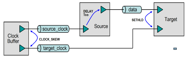
The basic equations that govern the setup and hold timing margin calculation include the delay (Tco) values of the driving chip, setup and hold constraints on the target chip, etch delays, and clock skews.
For more information, see Clock Skew in Synchronous Interface Timing.
Source-Synchronous Interface Timing
In a source-synchronous (clock-forwarded) interface, both the clock and data transmits from the same source device to the same target device.

These interfaces can clock off one (single-data-rate or SDR) or both edges (dual-data-rate or DDR) of the clock. The primary advantage of a source synchronous interface is that both the clock and data are driven from the same chip and typically routed on the same layers of the PCB at matched length. As a result, the effects of the device process, temperature, voltage variation, and interconnect variation become correlated. This reduces signaling skew and results in faster signaling rates.
You can specify the jitter (defined as cycle-to-cycle jitter) on the clock transfer nets. The specified jitter affects the hold margins.
In a dual data rate system, timing is relative to the rising and falling clock edges as well as the rising and falling data edges. As a result, there are total of eight margin calculations, four for setup and four for hold.
| Data R/F | Clock R/F | Margin | Equation |
|---|---|---|---|
| R | R | Setup |
RminC – RmaxD – RmaxDS – Rsetup |
| R | R | Hold |
UI + RminD + RminDS – RmaxC – Rhold – Jitter |
| R | F | Setup |
FminC – RmaxD – FmaxDS – Fsetup |
| R | F | Hold |
UI + RminD + FminDS – FmaxC – Fhold – Jitter |
| F | R | Setup |
RminC – FmaxD – RmaxDS – Rsetup |
| F | R | Hold |
UI + FminD + RminDS – RmaxC – Rhold – Jitter |
| F | F | Setup |
FminC – FmaxD – FmaxDS – Fsetup |
| F | F | Hold |
UI + FminD + FminDS – FmaxC – Fhold – Jitter |
Here, R refers to rising edge, F refers to falling edge, D refers to data etch delay, C refers to clock etch delay, DS refers to delay skews from the timing model for the driving device, setup refers to setup constraints from the timing model for the receiving device, hold refers to hold constraints from the timing model of the receiving device, UI refers to unit interval at the data transfer net, and Jitter refers to jitter defined in the clock transfer net.
Timing margin calculations are performed on a corner-by-corner basis. Cross corner interconnect delays for clock and data (e.g. FFFE and SSSE) are never combined to calculate setup and hold margins, as a given device cannot be both fast and slow simultaneously.
For more information, see Clock Skew in Source-Synchronous Interface Timing.
Clock Buffers and PLLs
The timing characteristics of a clock buffer include its intrinsic delay and skew between its output pins.
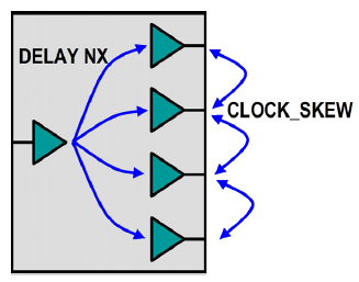
The Parallel Link Designer app models the intrinsic delay with the inverting
delay (DELAY IX) and non-inverting delay (DELAY NX)
timing model statements. It models the skew between the outputs with the
CLOCK_SKEW timing model statement.
For PLLs, there is an additional DELAY PLL statement in the timing
model which specifies the feedback path between the input and output pins.

When tracing through a clock buffer or PLL, the Parallel Link Designer app uses the delay timing statements to determine the connectivity between the transfer nets of the input and output. It must be able to do this in order to trace the complete clock path.
For more information, see Clock Delay Through Buffers and PLLs.
Pre-layout vs. Post-layout timing
In pre-layout timing analysis, a transfer net sheet is often used to represent an entire bus for an interface (data, address, or control). Each pin in this bus may have a unique set of timing parameters associated with it. For example, a source device may have pin-specific Tco values. The Parallel Link Designer app calculates the pre-layout and post-layout timing differently in this case.
During the pre-layout analysis, the app finds the minimum and maximum delay values for any bit involved in the transaction and use those delays for all bits in the bus. This provides a conservative estimate of timing margins.
During the post-layout analysis, the app analyzes the timing margins for each bit independently. It then combines the simulated etch delay the associated clock and data nets with pin-specific timing data. This provides a better estimate of the operating timing margin of the design.
Setting Up Timing Analysis
Synchronous Timing Setup
To setup the synchronous timing interface:
Create the data transfer net sheet of the type
DATA.Define the delay statements in the timing model. For single-data-rate (SDR) transfers, one delay statement is enough. For dual-data-rate (DDR) transfers, you must define two delay statements, one for the rising clock edge, the other for the falling clock edge.
To define a part with a clock-to-out from minimum 1 ns to maximum 3 ns on the
PINDEFgroupDATAwith respect to thePINDEFgroupCLK, use theDELAYstatement:DELAY R CLK *TO DATA 1.0 3.0
Define the setup and hold timing constraints between the data and the clock pin groups. For DDR, you need to
SETHLDstatements.To define a part with a setup requirement of 3 ns and a hold requirement of 1ns for the
PINDEFgroupDATAwith respect to thePINDEFgroupCLK, use theSETHLDstatement:SETHLD DATA *TO R CLK 3.0 1.0
To enable dynamic calculations of clock skew:
Create the appropriate transfer net sheets for the source and target clock. These sheets must be of type
CLOCKorSTROBE. The clocks/strobes must both originate from the same clock buffer device and connect to the clock pins of the clocked source and target devices.Add a
CLOCK_SKEWstatement in the timing model for the clock buffer between the output clock pin groups to define the drive uncertainty for these output pins.
To define a device with clock output
PINDEFgroupsCLK1andCLK2with a skew of ± 200 ps, use theCLOCK_SKEWstatement:.CLOCK_SKEW R CLK1 *TO CLK2 -0.2 0.2
Note
All output clock pins may be in the same PINDEF group. The
CLOCK_SKEW statement can reference the PINDEF to
itself.
Source-Synchronous Timing Setup
To setup the source-synchronous timing interface:
Create the appropriate transfer net sheets. In the simplest case, there must be two transfer net sheets, one for the data net and one for the clock net. The data transfer net sheet should be of type
DATAand the clock transfer net sheet should be of typeCLOCKorSTROBE.Add a
DELAY_SKEWstatement in the timing model for the driving chip between the data and clock pin groups. For DDR, you need twoDELAY_SKEWstatements.To define a device that has a ± 200 ps skew between the clock and data
PINDEFgroups, use theDELAY_SKEWstatement:DELAY_SKEW R clock *TO data -0.2 0.2
Add a
SETHLD(setup and hold) timing constraint defined between the data and clock pin groups in the timing model for the target chip. For DDR, you need twoSETHLDstatements.To define a part with a setup requirement of 3 ns and a hold requirement of 1 ns for the
PINDEFgroupDATAwith respect to thePINDEFgroupCLK, use theSETHLDstatement:SETHLD data *TO R clock 3.0 1.0
Timing Setup Through Clock Buffers
The Parallel Link Designer app supports timing through clock buffers for both synchronous and source-synchronous timing. To enable timing through a clock buffer:
Set up the basic Synchronous Timing Setup or Source-Synchronous Timing Setup for the data signals.
Create separate transfer net sheets of type
CLOCKorSTROBEfor the clocks into and out of the clock buffer. If the outputs of the clock buffer go to different target parts, you need to create a transfer net for each unique target part.Add a inverting or non-inverting delay statement in the timing model for the clock buffer between the input pin and the output pin groups.
To define a non-inverting clock buffer with a minimum delay of 500 ps and maximum delay of 2.5 ns between the input and output pins, use the
DELAY NXstatement:DELAY NX CKIN *TO CKOUT 0.500 2.500
Timing Setup Through PLL
The Parallel Link Designer app supports timing through PLLs, including the feedback path, for both synchronous and source-synchronous timing. You can also choose whether to simulate the feedback path. To enable timing through a PLL:
Set up the basic Synchronous Timing Setup or Source-Synchronous Timing Setup for the data signals.
Create separate transfer net sheets of type
CLOCKorSTROBEfor the clocks into and out of the clock buffer. If the outputs of the clock buffer go to different target parts, you need to create a transfer net for each unique target part.Create a transfer net sheet for the PLL feedback path of type
CLOCK. The source part and the target part is the PLL.Add a PLL delay statement in the timing model for the clock buffer between the feedback output pin and the feedback input pin groups.
To define a feedback path with a minimum delay of 250 ps and maximum delay of 350ps, use the
DELAY PLLstatement:DELAY PLL FBIN *TO FBOUT 0.250 0.350
Note
Any delay values derived from the simulation takes precedence over the values in the DELAY PLL statement.
Setup for Trained Timing
Trained timing is used by devices that align a clock or strobe with a data valid
window by delaying the clock or strobe using a DLL. The timing model requires a
TRAINED statement to specify the DLL parameters for the pin groups
for a clock or strobe.
Consider a controller timing model with a DQ and DQS pin group that has
DELAY_SKEW statements:
DELAY_SKEW R DQS1 *TO DQ1 DQ_SKEW_MIN DQ_SKEW_MAX
DELAY_SKEW F DQS1 *TO DQ1 DQ_SKEW_MIN DQ_SKEW_MAX
The TRAINED statements for the pin group DQS1 is:
TRAINED_DELAY_SKEW DQS1 MIN_TAP_INC MAX_TAP_INC TAP_GRAN
The Waveform and Timing Report generated from the app shows the margin without training, the optimal sample time, and the DLL tap that give margins closest to the optimal margins in the Training Details tab.
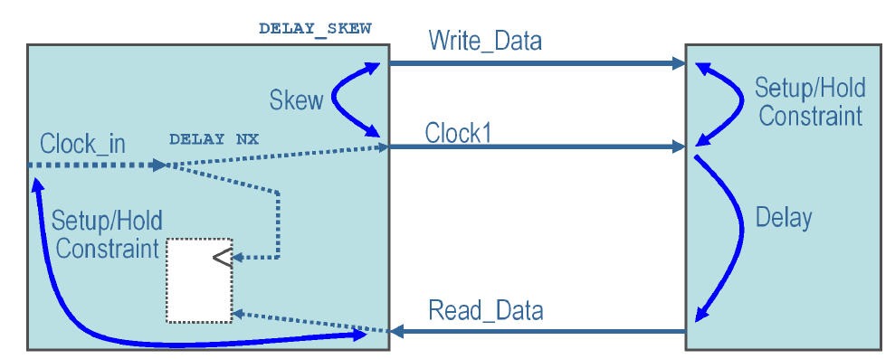
Setup for External Loop Clock
In an external loop clock system, a controller generates a read and write clock and the read clock is looped back to the controller. In this system writes (Controller to Memory) are source-synchronous and reads (Memory to Controller) are synchronous.

The controller needs a DELAY_SKEW statement for the Clock1 to
Write_Data relationship.
DELAY_SKEW R Clock1_out *TO Write_Data SKEW_MIN SKEW_MAX
CLOCK_SKEW Clock1_out *TO Clock2_out SKEW_MIN SKEW_MAX
SETHLD Read_Data *TO R Clock2_in SETUP HOLD
The memory timing model needs a DELAY statement for the Clock1 to
Read_Data timing relationship.
DELAY R Clock1_in *TO Read_Data DELAY_MIN DELAY_MAX
SETHLD Write_Data *TO R Clock2_in SETUP HOLD
Setup for Internal Loop Clock
In an internal loop clock system, the clock for the read data is internal to the controller. The read and write timing is the similar as in the external case.

The data sheet timing references the setup and hold of the read data to Clock1, the
output clock from the controller. The Parallel Link Designer app still requires
an input clock for the setup and hold constraint for read data at the controller, so you
must create a dummy input clock. This dummy input clock has a DELAY NX
statement with zero delay to Clock1, so it has the same timing as Clock1.
The dummy input clock pin can be an existing unused clock pin in the IBIS file.
Alternatively, you can add a pin to the IBIS component and timing model
PINDEF. The dummy input clock does not require any transfer net. It
is only used to create a common reference point for the synchronous timing calculation for
data reads.
The controller needs a DELAY_SKEW statement for the Clock1 to
Write_Data relationship.
DELAY_SKEW R Clock1_out *TO Write_Data SKEW_MIN SKEW_MAX
DELAY NX Clock1_in *TO Clock1_out 0
SETHLD Read_Data *TO R Clock_in SETUP HOLD
The memory timing model needs a DELAY statement for the Clock1 to
Read_Data timing relationship.
DELAY R Clock1_in *TO Read_Data DELAY_MIN DELAY_MAX
SETHLD Write_Data *TO R Clock2_in SETUP HOLD
Timing Report
You can access the results of the timing analysis from the Waveform and Timing Report. To launch the report, click Reports > Waveform and Timing Report. The report contains multiple tabs with timing data. For more information, see Timing Analysis Reports.
| Tab | Description |
|---|---|
| Timing Report Log | Syntax errors and summary of edge details described in the Edge Details tab. |
| Timing | Combines the rising edge and falling edge data described in the By Edge tab. |
| By Transfer | Combines the identical transfers (same driver and receiver) described in the By Variation tab. |
| By Variation | Combines the rising edge variation and falling edge variation data described in the By Edge Variation tab. |
| By Variation Details | Contains the setup and hold margins for both rising and falling edges at each receiver in each simulation. |
| By Variation Details Summary | Contains two rows for each transfer net: one for the smallest setup margin and the other for the smallest hold margin. |
| Timing Waveform Margin Details | Summarizes both waveform and timing information across each simulation in a single tab. |
| By Driver | Combines the identical drivers described in the By Variation tab. |
| By Receiver | Combines the identical receivers described in the By Variation tab. |
| Synchronous Details | Contains the timing data for nets using a regular (centralized) clocking configuration by receiver. It includes setup and hold margins and etch delays referenced to driver test load. It also lists receiver setup and hold time specs, driver clock to out delays, UI (bit time), and clock skews used to calculate the margins. |
| Source Synchronous Details | Contains the timing data for nets using a source synchronous clock, by receiver. It includes setup and hold margins as well as data and clock etch delays referenced to driver test load. It also lists receiver setup and hold time specs, UI (bit time), and driver skews used to calculate the margins. |
| Clock Buffer Details | Shows the non-inverting delays and feedback etch delays for clock buffers. |
| Clock Path Details | Contains the details of the etch delay calculation for clock paths that traverse buffers or PLLs. This includes the etch delay of the PLL output, etch delay of the PLL feedback, and non-inverting delay of the PLL for each process corner run. |
| Training Details | Contains the data showing the setup and hold margins without training (Untrained Setup/Hold Margin), the setup and hold margins if the tap could be set to any value (Optimal Setup/Hold Margin), and the setup and hold margin when the taps are set to there best setting (Trained Setup/Hold Margin). The tap used for the best setting and the delay from that tap are reported as well as the transfer net, pin group (from the timing model) and the type of training statement (from the timing model). |
| Edge Details | Summarizes data on each edge in each simulation. |
| Timing Waveform Margin | Contains the timing and waveform margin results. |
| Coupling Pushout (SSO mode only) | Reports the coupling effects on timing. |
| Coupling Noise (SSO mode only) | Reports the voltage variation on victim nets caused by coupling. |