Monitor and Analyze Applications Targeted to AMD RFSoC Devices
This example shows how to monitor, analyze, and debug a single channel of the analog-to-digital converter (ADC), digital-to-analog converter (DAC), and valid signals of the AXI4-Stream interface of the RF Data Converter block. This example uses the Simulink® model from the Transmit and Receive Tone Using AMD RFSoC Device - Part 2 Deployment example and integrates FPGA data capture from HDL Verifier™ to capture the required data.
Introduction
Monitoring IP core internal signals while a design is running on real hardware is useful because it allows you to debug and analyze the design. This example shows how to use FPGA data capture to capture internal signals of the generated DUT in MATLAB®. You use the FPGA Data Capture tool to capture the hardware signals over JTAG for debugging and analysis. FPGA data capture offers many capabilities to capture signals of interest using appropriate trigger and capture conditions. For more information on data capture modes and trigger options, see Data Capture Workflow (HDL Verifier) and FPGA Data Capture Component Generator (HDL Verifier).
Supported Hardware Platforms
AMD® Zynq® UltraScale+™ ZCU111 Evaluation kit + XM500 balun card
Generate FPGA Data Capture Components
Start the FPGA Data Capture Component Generator tool by executing this command in MATLAB in the current working directory.
generateFPGADataCaptureIP
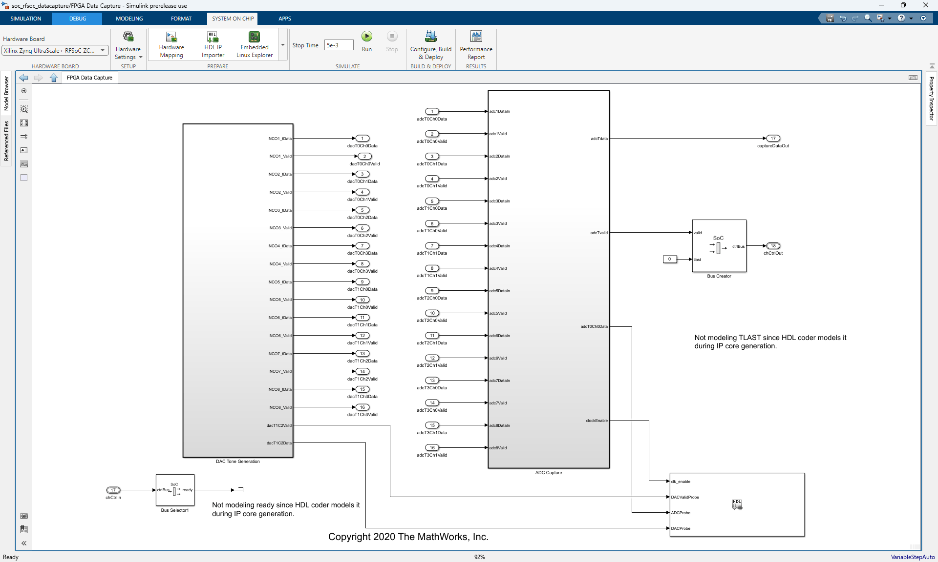
This example monitors three signals from the Transmit and Receive Tone Using AMD RFSoC Device example: dacT1Ch2, adcT0Ch0, and dacT1Ch2Valid. The dacT1Ch2 signal is 64 bits wide and consists of 4 samples of the real signal generated from NCO. The dacT1Ch2 signal drives the DAC ports of the RF Data Converter block in the transmit path. The adcT0Ch0 signal is the output of the RF Data Converter block and drives the capture logic in the DUT on the receive path. The dacT1Ch2Valid signal is a valid signal generated by the DAC Tone Generation DUT. In this example, you tap 16 bits of the dacT1Ch2 signal and 1 bit of the dacT1Ch2Valid signal from the DAC Tone Generation DUT, and 16 bits of the adcT0Ch0 signal from the ADC Capture DUT. You connect these signals to corresponding signals in the custom debugCore Simulink block, which integrates the data capture IP.
Set these parameters in the FPGA Data Capture Component Generator tool.
Navigate to the Target pane.
Set FPGA vendor to
AMD.Set Number of data capture IPs to
1.Set Connection type to
JTAG. (SoC Builder workflow supports the JTAG connection only).Set Generated IP language to
Verilog.Use the Browse button to select the project folder. The default folder name is
hdlsrc.Navigate to Ports pane in the Data Capture 1 tab.
Add two additional rows to the Ports table by clicking the Add button twice.
Rename the first signal in the Port Name field to
DACValidProbe, change the Bit Width field to1, and select Both trigger and data in the Use As field .Rename the second signal in the Port Name field to
ADCProbe, change the Bit Width to16, and select Data from the Use As field drop-down list.Rename the third signal in the Port Name field to
DACProbe, change the Bit Width to16, and select Data from the Use As field drop-down list.Navigate to the Capture pane.
Set Storage type to
Internal memoryto store captured data in the BRAM resources of the FPGA (SoC Builder workflow supports the internal memory storage type only).Set Sample depth to
4096. This value is the number of samples of each signal that the data capture tool returns to MATLAB each time a trigger is detected.Set Max trigger stages to
1. This value is the maximum number of trigger stages that you can add during data capture to provide multiple trigger conditions.Click Generate to generate the FPGA data capture IP in the current working folder. Observe the Messages pane to see total memory used by the data capture IP for capturing the selected signals.
Run the
helperDebugCoreIntegration.mhelper file in MATLAB to include the JTAG BSCAN IP.

Create Custom Simulink Block for Generated Data Capture IP
Follow these steps to create a Simulink block from the FPGA data capture IP.
1. Launch the HDL IP Importer by executing the hdlIPImporter command in MATLAB.
2. In the Enter Block Details window, specify block name and library name as debugCore. Specify the library location or browse to the project folder by using the Browse button to select the folder to create the block.
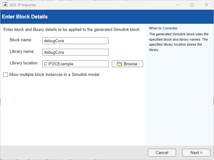
3. Clear the Allow multiple block instances in a Simulink model check box because this example uses only one block instance. Click Next to proceed.
4. In the Select HDL IP Source Location window, select Specify HDL IP source location and specify the IP location for the generated data capture IP.
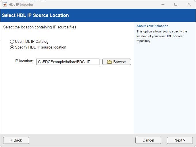
5. Click Next to proceed.
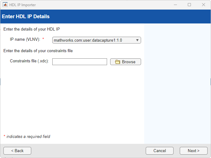
6. In the Enter HDL IP Details window, the tool automatically detects the FPGA data capture IP from the repository and displays it the IP Name(VLNV) field.
7. Leave Constraints file(.xdc) empty as there is no XDC file. Click Next.
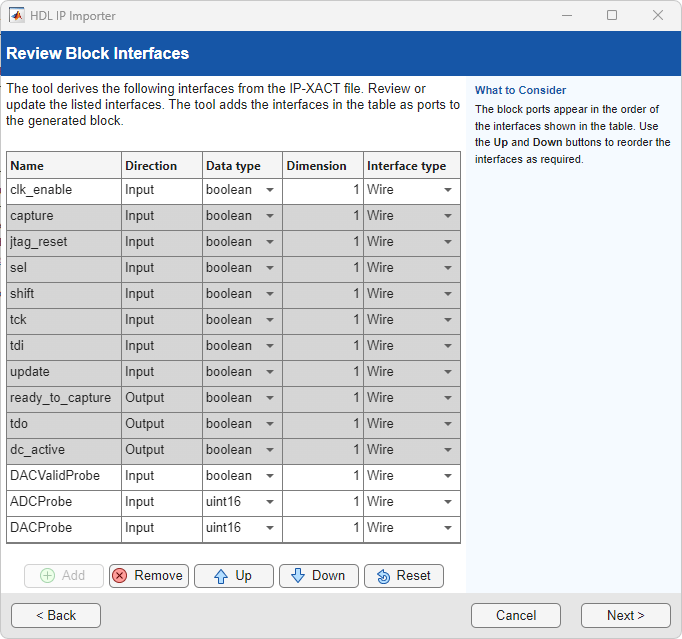
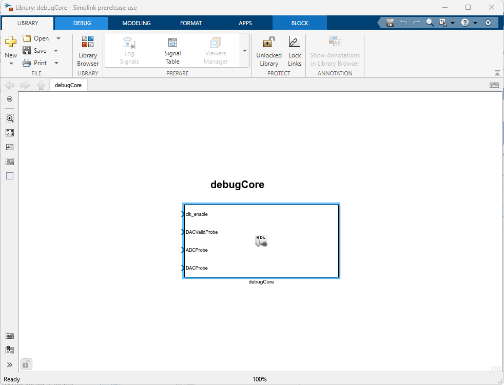
8. The Review Block Interfaces window lists all the interfaces on the block. The required ports for the debugCore block are ADCProbe, DACProbe, DACValidProbe, and clk_enable. Select the interfaces that are not required on the block and click Remove to remove them. Set the data type of the ADCProbe and DACProbe ports to int16.
9. In the Review Clock and Reset Interfaces window, the tool displays the clock interface required for the IP. Click Next to proceed.
10. In the Enter Linux Device Details window, click Next since there is no associated Linux driver with this block.
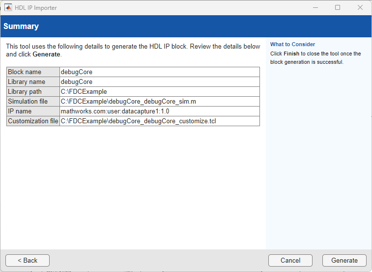
11. In the Summary window, review the details in the table and click Generate to generate the Simulink block.
12. After the block is generated, you can see a model with the created block.
Integrate Custom Simulink Block into Test Model
This example uses the Transmit and Receive Tone Using AMD RFSoC Device example model to integrate the debugCore block and monitor signals.
1. Run the following command in MATLAB in the current working directory to integrate the JTAG debug IP with the debugCore IP. Change the destination file name if you use a different name for the library block.
copyfile('integrateJTAGDebugCore.tcl','debugCore_debugCore_customize.tcl','f')
2. Open the soc_rfsoc_datacapture model from the Transmit and Receive Tone Using AMD RFSoC Device example in MATLAB by typing this command in the command window.
soc_rfsoc_datacapture
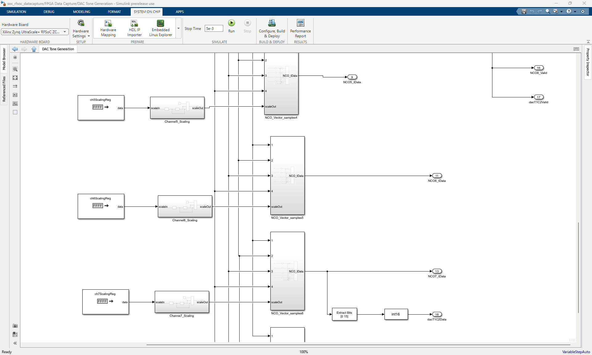
3. Open the soc_rfsoc_datacapture_fpga FPGA model. Inside the DAC Tone Generation DUT, create a new output port and name it dacT1Ch2DataProbe.
4. Connect the NCO7_tData output port in the DAC Tone Generation DUT signal to the dacT1Ch2DataProbe output port through an Extract bits block followed by a Cast block.
5. Configure the Extract bits block to extract the LSB 16 bits of the signal. Configure the Cast block to convert the output data type to int16.
7. Similarly, create a new output port for the DAC Tone Generation DUT and name it dacValidProbe.
8. Connect the Valid output port to the dacValidProbe port of the DAC Tone Generation DUT.
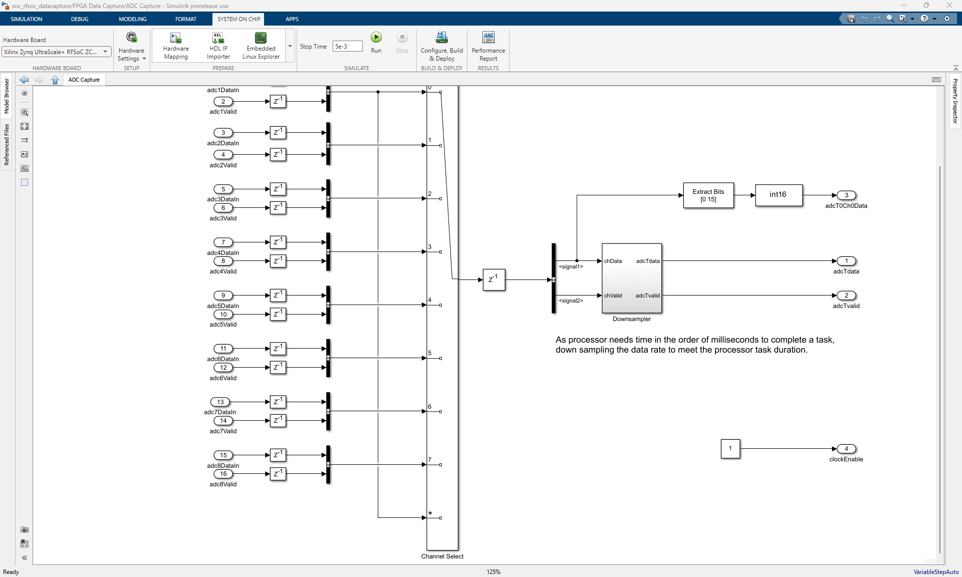
9. Inside the ADC Capture DUT, create a new output port and name it adcT0Ch0DataProbe.
10. Connect the bus selector output signal1 in the ADC Capture DUT to the adcT0Ch0DataProbe output port through an Extract bits block followed by a Cast block.
11. Configure the Extract bits block to extract the LSB 16 bits of the signal, and configure the Cast block to convert the output data type to int16.
12. Inside the ADC Capture DUT, create a new output port and name it clockEnable. Instantiate a Constant block, configure its output to 1, and set Output data type to boolean in the Signal Attributes tab. Connect the Constant block output to the clockEnable output port.
13. Copy the generated debugCore Simulink block into the soc_rfsoc_datacapture_fpga FPGA model.
14. Connect the dacT1Ch2DataProbe output port of DAC Tone Generation DUT to the DACProbe input port of the debugCore block.
15. Connect the dacValidProbe output port of DAC Tone Generation DUT to the DACValidProbe input port of the debugCore block.
16. Connect the adcT0Ch0DataProbe output port of ADC Capture DUT to the ADCProbe input port of the debugCore block.
17. Connect the clockEnable output port of ADC Capture DUT to the clk_enable input port of the debugCore block.
Implement and Deploy Model
For steps on implementing, building, deploying, and testing the model on the AMD RFSoC device, see the Transmit and Receive Tone Using AMD RFSoC Device - Part 2 Deployment example. When you deploy the bitstream onto the hardware and the software model is running in external mode, you can follow the FPGA data capture process to capture the data seen by the probes of the debugCore block.
Capture and Display Data from FPGA Data Capture IP
Locate the FPGA Data Capture launch script launchDataCaptureApp.m in the FDC_IP directory. Add the FDC_IP directory to the MATLAB path and run the launchDataCaptureApp script in MATLAB.
1. On the Trigger tab, select DACValidProbe as the trigger signal and select the Operator as == and Value as High.
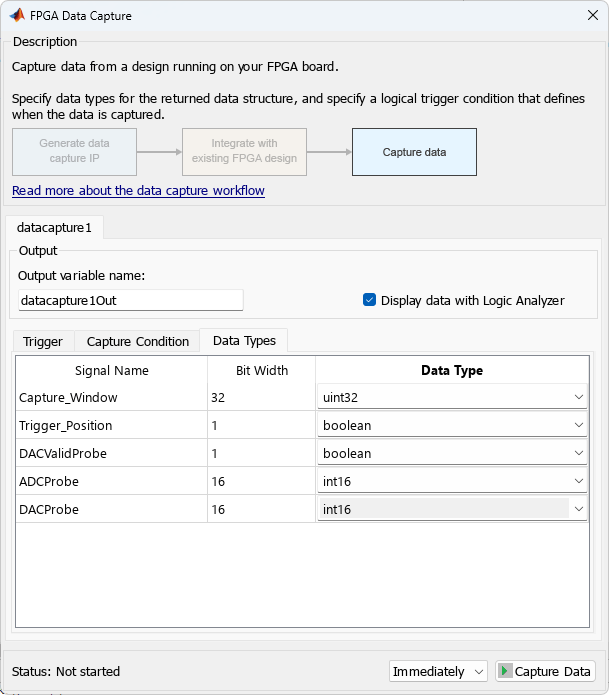
2. Select the Data Types tab and change the Data Type fields of the DACProbe and ADCProbe signals to int16.
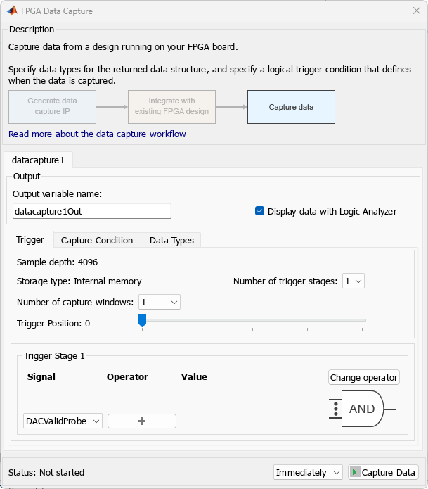
3. Click Capture Data to start the ADC and DAC data capture and display it in Logic Analyzer.
3. In the Logic Analyzer app, navigate to the Wave tab, in the Name field, select DACProbe and set the format to Analog. Repeat this step for the ADCProbe signal. You can now view the captured DACProbe, ADCProbe, and dacValidProbe signals in Logic Analyzer.

4. You can trigger the capture again by clicking the Capture Data button in FPGA Data Capture application.
Summary
In this example, you import the FPGA data capture IP from HDL Verifier by using the HDL IP Importer and integrate it into an SoC Blockset design. You integrate the FPGA data capture IP into the Transmit and Receive Tone Using AMD RFSoC Device example to monitor and analyze signals inside the RFSoC device while running the model on hardware. You verify that the system works as expected on the hardware by monitoring the captured signals from the FPGA data capture IP. You can use this mechanism to debug signals in any model targeted for any of the supported AMD SoC hardware in SoC Blockset.
See Also
HDL IP Importer | FPGA Data Capture Component Generator (HDL Verifier) | FPGA Data Capture (HDL Verifier)
Topics
- Import HDL IP Core into SoC Model
- Data Capture Workflow (HDL Verifier)