Thyristor-Based HVDC Link
Description of the HVDC Transmission System
The example in this section illustrates modeling of a high-voltage direct current (HVDC) transmission link using 12-pulse thyristor converters [1]. Perturbations are applied to examine the system performance. The objectives of this example are to demonstrate the use of Simscape™ Electrical™ Specialized Power Systems blocks in combination with Simulink® blocks in the simulation of a complete pole of a 12-pulse HVDC transmission system.
Open the Thyristor-Based HVDC Transmission System model and save it under a different name to allow further modifications to the original system.
A 1000 MW (500 kV, 2 kA) DC interconnection is used to transmit power from a 500 kV, 5000 MVA, 60 Hz system to a 345 kV, 10000 MVA, 50 Hz system. The AC systems are represented by damped L-R equivalents with an angle of 80 degrees at fundamental frequency (60 Hz or 50 Hz) and at the third harmonic.
The rectifier and the inverter are 12-pulse converters using two Universal Bridge blocks connected in series. The converters are interconnected through a 300-km line and 0.5 H smoothing reactors. The converter transformers (Wye grounded/Wye/Delta) are modeled with Three-Phase Transformer (Three-Windings) blocks. The transformer tap changers are not simulated. The tap position is rather at a fixed position determined by a multiplication factor applied to the primary nominal voltage of the converter transformers (0.90 on the rectifier side; 0.96 on the inverter side).
From the AC point of view, an HVDC converter acts as a source of harmonic currents. From the DC point of view, it is a source of harmonic voltages.
The order n of these characteristic harmonics is related to the pulse number p of the converter configuration: n = kp ± 1 for the AC current and n = kp for the direct voltage, k being any integer. In the example, p = 12, so that injected harmonics on the AC side are 11, 13, 23, 25, and on the DC side are 12, 24.
AC filters are used to prevent the odd harmonic currents from spreading out on the AC system. The filters are grouped in two subsystems. These filters also appear as large capacitors at fundamental frequency, thus providing reactive power compensation for the rectifier consumption due to the firing angle α. For α = 30 degrees, the converter reactive power demand is approximately 60% of the power transmitted at full load. The AC filters subsystem contains the high Q (100) tuned filters at the 11th and 13th harmonics and the low Q (3), or damped filter, used to eliminate the higher order harmonics, e.g., 24th and up. Extra reactive power is also provided by capacitor banks.
Two Breaker blocks apply faults on the rectifier DC side and on the inverter AC side to examine system performance.
The power system and the control and protection system are both discretized with the same sample time Ts = 50 µs. Some protection systems have a sample time of 1 or 2 ms.
Frequency Response of the AC and DC Systems
The section Analyze a Simple Circuit explains how you can use the Impedance Measurement block to compute the impedance of a linear system from its state-space model. As the thyristor valves of the converters are nonlinear blocks, they are ignored in the impedance calculation and you get the impedances with the valves open.
The rectifier and inverter subsystems use Impedance Measurement blocks to measure the frequency response between phase A and phase B of the AC systems. Measuring the impedance between two phases gives two times the positive-sequence impedance. Therefore you specify a multiplication factor of 1/2 on the Impedance Measurement blocks to obtain the correct impedance value. The ZDC Impedance Measurement block measures the impedance on the DC line rectifier terminal side.
You can use the Impedance vs Frequency Measurement tool of Powergui to display the magnitude and phase as a function of frequency measured by the three Impedance Measurement blocks..
The magnitudes of the three impedances as a function of frequency are shown here.
Positive-Sequence Impedances of the Two AC Systems and of the DC Line
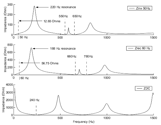
Note the two minimum impedances on the Z magnitudes of the AC systems. These series resonances are created by the 11th and 13th harmonic filters. They occur at 660 Hz and 780 Hz on the 60 Hz system. Note also that the addition of 600 Mvar capacitive filters on the inductive systems creates resonances around 188 Hz on the rectifier side and 220 Hz on the inverter side. In the 60 Hz region, the magnitude is 56.75 Ω for the 60 Hz system, corresponding to an effective short-circuit level of 5002/56.75 = 4405 MVA on the rectifier side (5000 MVA - 600 Mvar of filters).
For the DC line, note the series resonance at 240 Hz, which corresponds to the main mode likely to be excited on the DC side, under large disturbances.
Control and Protection Systems
The Rectifier Pole Control (Current) and the Inverter Pole Control (Current/Voltage/Gamma) subsystems generate the current reference for both converters and initiates the starting and stopping of the DC power transmission. At the inverter, the Gamma Measurement subsystem measures the extinction angle Gamma of the 6-pulse thyristor converters.
The protection systems can be switched on and off. At the rectifier, the DC fault protection detects a fault on the line and takes the necessary action to clear the fault. The Low AC Voltage Detection subsystem at the rectifier and inverter serves to discriminate between an AC fault and a DC fault. At the inverter, the Commutation Failure Prevention Control subsystem [2] mitigates commutation failures due to AC voltage dips.
Synchronization and Firing System
The synchronization and generation of the 12 firing pulses is performed by the 12-Pulse Firing Control system. This system uses the primary voltages to synchronize and generate the pulses according to the alpha firing angle computed by converter controller. The synchronizing voltages are measured at the primary side of the converter transformer because the waveforms are less distorted. A Phase Locked Loop (PLL) is used to generate three voltages synchronized on the fundamental component of the positive-sequence voltages. The firing pulse generator is synchronized to the three voltages generated by the PLL. At the zero crossings of the commutating voltages (AB, BC, CA), a ramp is reset. A firing pulse is generated whenever the ramp value becomes equal to the desired delay angle provided by the controller.
Steady-State V-I Characteristic
The Rectifier Pole Control and the Inverter Pole Control subsystems implement this steady-state characteristic:
Rectifier and Inverter Steady-State Characteristics and VDCOL Function
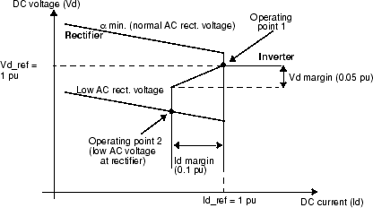
In normal operation, the rectifier controls the current at the
Id_ref reference value, whereas the inverter controls the
voltage or gamma at the Vd_ref or
Gamma_min reference value.
The system normally operates at point 1 as shown in the figure. However, during a severe contingency producing a voltage drop on the AC system 1 feeding the rectifier, the operating point moves to point 2. The rectifier, therefore, is forced to a minimum α mode and the inverter is in current control mode. Similarly, a voltage drop on the AC system feeding the inverter will force a control mode change to Gamma regulation to limit the angle to γ min. During severe contingency, a faster response is necessary to increase the commutation margin and consequently to reduce the probability of a commutation failure. The Commutation Failure Prevention Control subsystem (look under the Inverter protections block) generates a signal that decreases the maximum limit of the delay angle during the voltage drop (e.g., during an AC fault).
Note
γ = extinction angle = 180º - α - µ , µ = commutation or overlap angle
VDCOL Function
Another important control function is implemented to change the reference
current according to the value of the DC voltage. This control, named Voltage Dependent Current Order Limiter (VDCOL), automatically
reduces the reference current (Id_ref) set point when
VdL decreases (as, for example, during a DC line fault or
a severe AC fault). Reducing the Id reference currents also
reduces the reactive power demand on the AC system, helping to recover from
fault. The VDCOL parameters are explained by this diagram:
VDCOL Characteristic; Id_ref = f(VdL)
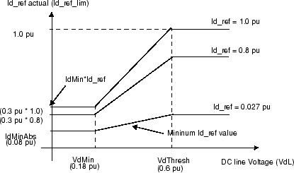
The Id_ref value starts to decrease when the Vd line
voltage falls below a threshold value VdThresh. The actual
reference current used by the controllers is available at the second controller
output, named Id_ref_lim. IdMinAbs is the
absolute minimum Id_ref value. When the DC line voltage falls
below the VdThresh value, the VDCOL drops instantaneously to
Id_ref. However, when the DC voltage recovers, VDCOL
limits the Id_ref rise time with a time constant defined by
parameter Tup.
Current, Voltage, and Gamma Regulators
Both rectifier and inverter controls have current regulator calculating firing
αi. At the inverter, operating in parallel with the
current regulator are the voltage and/or gamma regulators calculating firing
angles αv and/or αg. The effective
α angle is the minimum value of
αi, αv
and/or αg. All regulators are of the
proportional- integral type. They should have high enough gains for low
frequencies (<10 Hz) to maintain the current, voltage, or gamma response
equal to the reference current (Id_ref_lim), reference
voltage (Vd_ref), or reference gamma
(Gamma_min), as long as α is within the minimum and
maximum limits (5º < α < 166º for rectifier, 92º < α < 166º for
inverter). As described before, a signal (D_alpha) received from the Commutation
Failure Prevention protection can temporarily reduce the 166º limit at the
inverter. The regulator gains Kp and Ki are adjusted during small perturbations
in the reference.
Another particularity of the regulator is the linearization of the
proportional gain. As the Vd voltage generated by the
rectifier and the inverter is proportional to cos(α), the ΔVd variation due to a
Δα change is proportional to sin(α). With a constant Kp value, the effective
gain is, therefore, proportional to sin(α). To keep a constant proportional
gain, independent of the α value, the gain is linearized by multiplying the Kp
constant by 1/sin(α). This linearization is applied for a range of α defined by
two limits specified in the Rectifier and Inverter Pole
Control blocks.
System Startup/Stop — Steady-State and Step Response
The system is programmed to start and reach a steady state. Then a step is applied first to the reference current and later to the voltage reference so you can observe the dynamic response of the regulators. Finally, a stop sequence is initiated to bring the power transmission smoothly down before blocking the converters. Notice in the Converter Controller that after reception of the Stop signal a Forced_alpha is ordered for 0.150 s, and then 0.1 s later the blocking of the pulses is ordered.
Start the simulation and observe the signals on the Rectifier and Inverter scopes. The waveforms are reproduced here:
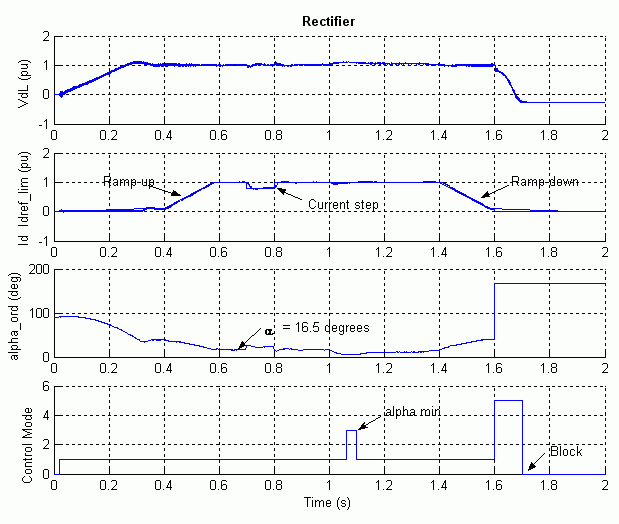
Startup/Stop of the DC System and Step Applied on the Current and Voltage Reference
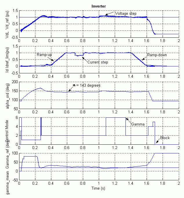
In the Master Control, the converters pulse generators are deblocked and the power
transmission started by ramping the reference current at t = 20 ms. The reference
reaches the minimum value of 0.1 pu in 0.3 s. Observe that the DC current starts to
build and the DC line is charged at its nominal voltage. At t = 0.4 s, the reference
current is ramped from 0.1 to 1 pu (2 kA) in 0.18 s (5 pu/s). The DC current reaches
steady state at the end of the starting sequence at approximately 0.58 s. The
rectifier controls the current and the inverter controls the voltage. Trace 1 of
both Rectifier and Inverter scopes shows the DC line voltage (1 pu = 500 kV). At the
inverter, the voltage reference is also shown. Trace 2 shows the reference current
and the measured Id current (1 pu = 2 kA). During the ramp, the
inverter is actually controlling the current (Trace 4: Mode = 1) to the value of
Id_ref_lim less the Current Margin (0.1 pu) and the rectifier
tries to control the current at Id_ref_lim. At the inverter, the
control mode changes from current control to gamma control (Mode = 6) before
stabilizing to voltage control (Mode = 2) at t = 0.3 s. The rectifier becomes
thereafter in control of the current. However, a control mode change will occur and
alpha is limited to the minimum value of 5 degrees (Mode = 3) during an increase of
the DC voltage initiated by a voltage reference increase at the inverter, as
explained in the next paragraph. At steady state (measured at t between 1.3 and 1.4
s), the α firing angles are around 16.5 degrees and 143 degrees respectively on the
rectifier and inverter side. The inverter control measures the extinction angle γ
for each thyristor of the two six-pulse bridges (i.e., the bridge connected to the
Wye and Delta windings) by determining the elapsed time expressed in electrical
degrees from the end of current conduction to the zero crossing of the commutating
voltage. The mean value of the measured gamma for the last 12 extinctions (6 of the
Delta converter and 6 of the Wye converter) is shown in traces 5 along with Gamma
reference. In steady state, the mean γ is around 22.5 degrees.
At t = 0.7 s, a -0.2 pu step is applied during 0.1 s to the reference current so that you can observe the dynamic response of the regulators. Later on, at t = 1.0 s, a 0.1 pu step is applied during 0.2 s at the inverter reference voltage. Observe that at the inverter the extinction angle reaches the reference value (e.g., the minimum acceptable value) and that the Gamma regulator takes control at t around 1.1 s. At t around 1.3 s the voltage regulator retakes control of the voltage.
At t = 1.4 s the Stop sequence is initiated by ramping down the current to 0.1 pu. At t = 1.6 s a Forced-alpha (to 166 deg) at the rectifier extinguishes the current and at the inverter the Forced-alpha (to 92 deg with a limited rate) brings down the DC voltage due to the trapped charge in the line capacitance. At t = 1.7 s the pulses are blocked in both converters.
Comparison of Theory and Simulation Results in Steady State
The main equations governing the steady-state operation of the DC system are given here so that you can compare the theoretical values to the simulation results.
The following expression relates the mean direct voltage Vd of a 12-pulse bridge to the direct current Id and firing angle α (neglecting the ohmic losses in the transformer and thyristors):
where Vdo is the ideal no-load direct voltage for a six-pulse bridge:
Vc is the line-to-line RMS commutating voltage that is dependent on the AC system voltage and the transformer ratio.
Rc is the equivalent commutating resistance.
Xc is the commutating reactance or transformer reactance referred to the valve side.
The following rectifier parameters were used in the simulation.
The Vc voltage must take into account the effective value of the voltage on the 500 kV bus and the transformer ratio. If you look at the waveforms displayed on the AC_Rectifier scope, you find 0.96 pu when the direct current Id has reached its steady state (1 pu).
If you open the rectifier transformer dialog box, you find a multiplication factor of 0.90 applied to the primary nominal voltage. The voltage applied to the inverter is therefore boosted by a factor of 1/0.90.
Vc = 0.96 * 200 kV/0.90 = 213.3 kV
Id = 2 kA
α = 16.5º
Xc = 0.24 pu, based on 1200 MVA and 222.2 kV = 9.874 Ω
Therefore, this theoretical voltage corresponds well with the expected rectifier voltage calculated from the inverter voltage and the voltage drop in the DC line (R = 4.5 Ω) and in the rectifier smoothing reactor (R = 1 Ω):
The µ commutation or overlap angle can also be calculated. Its theoretical value depends on α, the DC current Id, and the commutation reactance Xc.
Now verify the commutation angle by observing the currents in two valves, for example, current extinction in valve 1 and current buildup in valve 3 of the Y six-pulse bridge of the rectifier. These signals are available in the VALVE13_RECT scope.
The waveforms illustrating two cycles are shown in the following figure. The measured commutation angle is 14 steps of 50 µs or 15.1º of a 60 Hz period. The resolution with a 50 µs time step is 1.1º; this angle compares reasonably well with the theoretical value.
Valve Voltage and Currents (Commutation from Valve 1 to Valve 3)

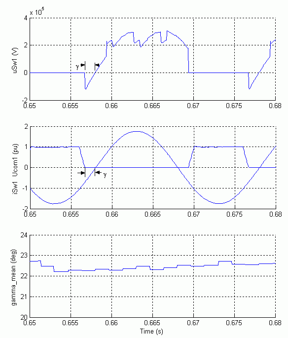
Finally, to validate the γ measurement at the inverter, observe the valve 1 voltage and current in the VALVE1_INV scope. Also observe the commutating voltage corresponding to the outgoing valve 1 to be extinguished and the mean value of γ as shown in Current and Commutation Voltage of Valve 1 Showing γ. Verify also that the values of α, µ, and γ add up to 180º.
Current and Commutation Voltage of Valve 1 Showing γ
DC Line Fault
Deactivate the steps applied on the current reference and on the voltage reference in the Master Control and in the Inverter Control and Protection respectively by setting the switches in lower position. In the DC Fault block, change the multiplication factor of 100 to 1, so that a fault is now applied at t = 0.7 s. Reduce the Simulation Stop time to 1.4 s. Open the Rectifier scope as well as the Fault scope to observe the fault current and the Protection Rectifier scope to observe the DC Fault protection action. Restart the simulation.
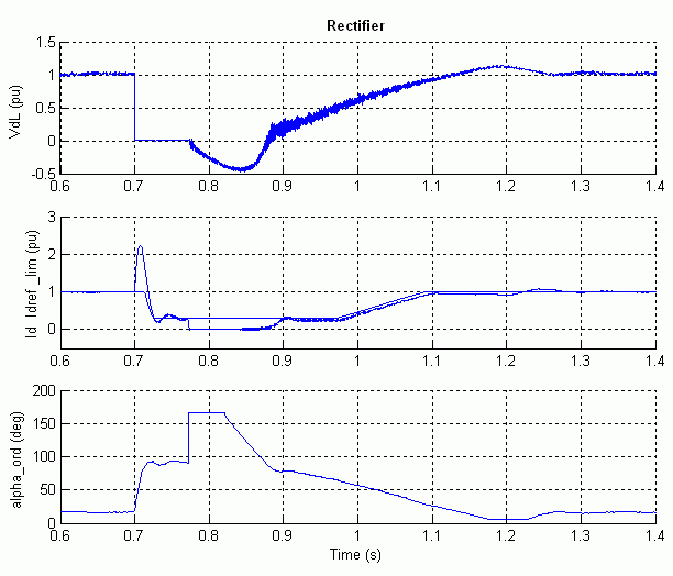
DC Line Fault on the Rectifier Side

At fault application (t = 0.7 s), the DC current increases to 2.2 pu and the DC voltage falls to zero at the rectifier. This DC voltage drop is seen by the Voltage Dependent Current Order Limiter (VDCOL) and the DC Fault protection. The VDCOL reduces the reference current to 0.3 pu at the rectifier. A DC current still continues to circulate in the fault. Then, at t = 0.77 s, the rectifier α firing angle is forced to 166 degrees by the DC Fault protection after detecting a low DC voltage. The rectifier now operates in inverter mode. The DC line voltage becomes negative and the energy stored in the line is returned to the AC system, causing rapid extinction of the fault current at its next zero crossing. Then α is released at t = 0.82 s and the normal DC voltage and current recover in approximately 0.5 s. Notice, the temporary mode change in the Rectifier controls between 1.18 s and 1.25 s.
AC Line-to-Ground Fault at the Inverter
Now modify the fault timings to apply a line-to-ground fault. In the DC Fault block, change the multiplication factor of 1 to 100, so that the DC fault is now eliminated. In the A-G Fault block, change the multiplication factor in the switching times to 1, so that a six-cycle line-to-ground fault is now applied at t = 0.7 s at the inverter. Restart the simulation.
Rectifier, Inverter Signals for an AC Line Fault on Inverter Side

Voltages and Currents on the 50 Hz Side for an AC Line Fault on the Inverter Side
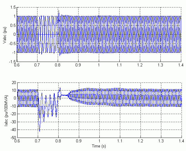
Notice the 120 Hz oscillations in the DC voltage and currents during the fault. An unavoidable commutation failure occurs at the inverter at the very beginning of the fault and the DC current increases to 2 pu. A commutation failure is the result of a failure of the incoming valve to take over the direct current before the commutation voltage reverses its polarity. The symptoms are a zero DC voltage across the affected bridge causing an increase of the DC current at a rate determined mainly by the DC circuit inductance. When the fault is cleared at t = 0.8 s, the VDCOL operates and reduces the reference current to 0.3 pu. The system recovers in approximately 0.35 s after fault clearing.
Look at the waveforms displayed on the PROTECTION INVERTER scope. The Low AC Voltage block detects the fault and locks the DC Fault protection that in this case should not detect a DC fault even if the DC line voltage dips. Look at the Commutation Failure Prevention Control (CFPREV) output (A_min_I) which decreases the maximum delay angle limit to increase the commutation margin during and after the fault.
Now open the dialog box of the CFPREV block located inside the Inverter Protections subsystem and deactivate the CFPREV protection by deselecting the “ON State.” Restart the simulation. Notice the slightly different transient behavior during and after the fault.
References
[1] Arrilaga, J., High Voltage Direct Current Transmission, IEEE® Power Engineering Series 6, Peter Peregrinus, Ltd., 1983.
[2] Lidong Zhang, Lars Dofnas, “A Novel Method to Mitigate Commutation Failures in HVDC Systems,” Proceedings PowerCon 2002. International Conference on, Volume: 1, 13–17 Oct. 2002, pp. 51–56.
Select a Web Site
Choose a web site to get translated content where available and see local events and offers. Based on your location, we recommend that you select: United States.
You can also select a web site from the following list
Americas
- América Latina (Español)
- Canada (English)
- United States (English)
Europe
- Belgium (English)
- Denmark (English)
- Deutschland (Deutsch)
- España (Español)
- Finland (English)
- France (Français)
- Ireland (English)
- Italia (Italiano)
- Luxembourg (English)
- Netherlands (English)
- Norway (English)
- Österreich (Deutsch)
- Portugal (English)
- Sweden (English)
- Switzerland
- United Kingdom (English)
Asia Pacific
- Australia (English)
- India (English)
- New Zealand (English)
- 中国
- 日本Japanese (日本語)
- 한국Korean (한국어)